

- IBM pushes transistor density beneath the long-feared one-nanometer barrier
- NanoStack abandons flat chip layouts in favour of vertical transistor stacking
- The prototype delivered 50% extra efficiency throughout IBM laboratory testing phases
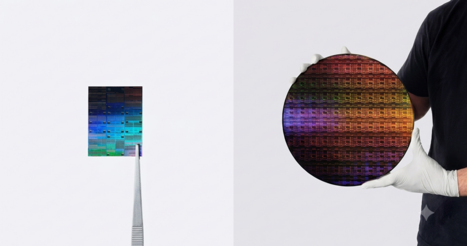
IBM has unveiled what it describes because the world’s first sub-1 nm chip know-how, carrying practically 100 billion transistors on a fingernail-sized floor.
The breakthrough revolves round a brand new 3D NanoStack structure that strikes transistor scaling into the 0.7 nm or 7 angstrom period.
For context, in the present day’s most superior business chips usually sit across the 2nm mark, making this a considerable leap in density.
Constructing upwards to maintain Moore’s Regulation alive
The semiconductor {industry} has spent a long time squeezing extra transistors onto more and more smaller items of silicon to enhance computing efficiency.
That course of has grow to be progressively more durable as transistor dimensions strategy the size of just a few atoms throughout fashionable processors.
IBM’s strategy avoids additional horizontal compression by stacking transistor layers vertically via a three-dimensional nanosheet structure as an alternative.
The design packs practically twice the transistor density of IBM’s 2 nm chip know-how launched again in 2021.
In keeping with the corporate, the structure additionally delivers roughly 40% larger SRAM scaling to assist more and more demanding AI workloads.
This vertical technique permits engineers to separate n-type and p-type transistors into distinct layers, which, in accordance with IBM, permits unbiased optimization of supplies for every.
, in contrast it with constructing an enormous block of flats fairly than homes in a metropolis.
“IBM’s NanoStack is like proposing a 100-storey skyscraper,” stated Professor Alan Woodward, a pc scientist at Surrey College.
Utilizing this analogy, IBM’s closest opponents, like Intel and Samsung, are someplace round a 30 to 50-storey constructing, a far cry from IBM.
In testing, the corporate reported a 50% efficiency enchancment and 70% larger vitality effectivity in contrast with its current 2nm chips, alongside a 40% acquire in on-chip reminiscence scaling.
Regardless of the quoted efficiency enhancements, the know-how stays years from business use, with IBM estimating manufacturing might start inside 5 years on the earliest.
“With our new NanoStack structure, we’re not simply making smaller transistors, we’re reinventing how chips are constructed to ship dramatically extra energy and vitality effectivity,” stated Jay Gambetta, Director of IBM Analysis and IBM Fellow.
The trade-offs behind the density features
Vertical stacking introduces problems largely round warmth dissipation, since transistors generate warmth that turns into more durable to handle when layered carefully collectively.
This identical tight spacing additionally raises the stakes for wafer alignment, since layers have to be bonded with excessive precision to keep away from malfunction.
Researchers acknowledge that when gaps between layers develop too skinny, transistors can fail to change off accurately, undermining the very density features NanoStack is supposed to ship.
These engineering trade-offs are signs of a deeper downside going through the whole chip {industry}.
For many years, producers have relied on Moore’s Regulation, the sample of transistor counts doubling roughly each two years.
However that tempo has grown more durable to maintain as designs strategy the bodily limits of particular person atoms.
Whether or not NanoStack genuinely extends that trajectory by one other decade, as IBM initiatives, depends upon whether or not these unresolved manufacturing challenges could be solved at scale.
It’s partly because of this that IBM has drawn in companions together with ASML, Lam Analysis, and Tokyo Electron, signalling an industry-wide effort behind this push towards angstrom-level scaling.
Even so, comparable daring claims accompanied IBM’s 2nm chip unveiling in 2021, however turning lab success into mass manufacturing traditionally takes longer than preliminary bulletins.
By way of IBM
Follow TechRadar on Google News and add us as a preferred source to get our professional information, opinions, and opinion in your feeds. Make sure that to click on the Comply with button!
And naturally it’s also possible to follow TechRadar on TikTok for information, opinions, unboxings in video type, and get common updates from us on WhatsApp too.