

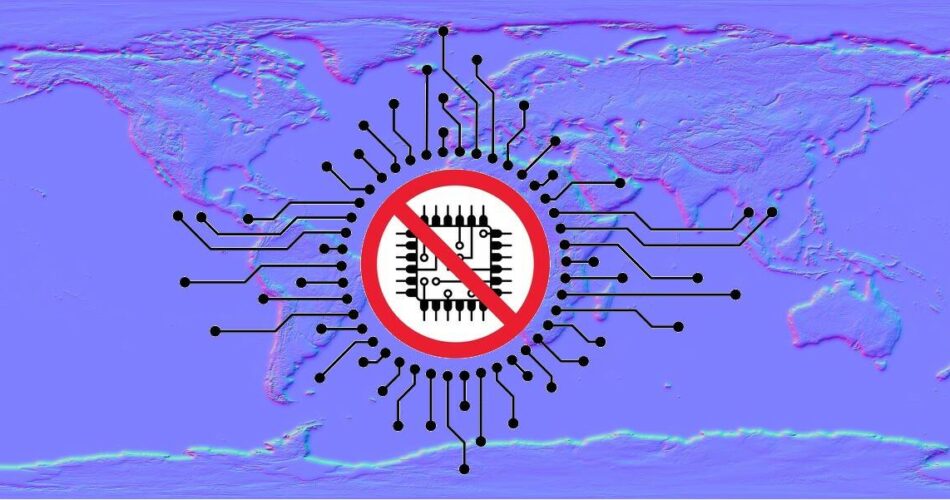
China’s primary semiconductor commerce group has launched a press release opposing the alliance between Japan, the Netherlands, and the US to limit chip exports to the nation.
“CSIA opposes the act of interfering in international commerce liberalization, distorting the stability of provide and demand,” stated the China Semiconductor Trade Affiliation.
The commerce org additionally alleged that the rationale the semiconductor trade is prospering in the present day is because of “international market and collaborative improvements” and the restrictions will “trigger critical hurt” to the trade in China, the worldwide financial system, and shopper curiosity worldwide.
It referred to as on Beijing and related businesses to ascertain guidelines for sustaining a “international semiconductor trade ecology.”
Talks to steer Japan and the Netherlands to hitch the US in bans on exporting chip expertise to China have been ongoing. By sanctions, the US has sought to forestall China from growing army expertise. The bans are additionally a protest in opposition to China’s human rights abuses.
Chinese language chipmakers like Yangtze Memory Technologies Corp (YMTC) and China’s largest foundry operator, SMIC, are already feeling the pinch.
Because the US just isn’t the one chip or associated tools maker on this planet, it grew to become essential for the nation to get buy-in from different nations.
Japan and the Netherlands are each on the forefront of chip tools manufacturing. The Netherlands’ ASML is the main maker of maximum ultraviolet (EUV) lithography machines, for which it already halted exports to China, and Japan’s Canon and Nikon make deep ultraviolet (DUV) lithography machines.
On the finish of January, the three nations reportedly got here to an settlement. However particulars of that settlement had been stored secret till an interview with a Japanese politician revealed that the nation is likely to be much less strict with its guidelines than the US.
In the meantime, Beijing has pondered a ban of its personal, doubtlessly for photovoltaic silicon wafer expertise. ®
Source link