

- Peking College transistor may outperform Intel, TSMC, and Samsung’s high silicon chips
- Full gate protection boosts pace and cuts power use in breakthrough Chinese language transistor design
- China could have simply leapfrogged US chip tech with this silicon-free transistor innovation
Chinese language researchers at Peking College have introduced what looks as if a breakthrough in transistor design, which if commercialized, may dramatically shift the course of microprocessor growth.
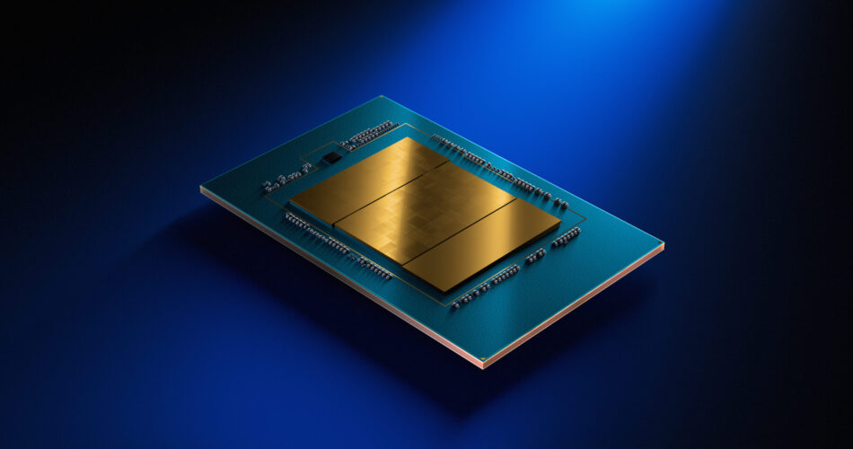
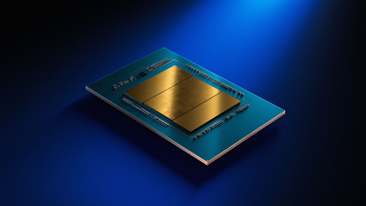
The workforce created a silicon-free transistor primarily based on a two-dimensional materials, bismuth oxyselenide.
The innovation hinges on the gate-all-around (GAAFET) structure, the place the transistor’s gate wraps utterly across the supply. Conventional FinFET designs, which dominate present silicon-based processors, solely enable partial gate protection. This full-wrap construction enhances the contact space between the gate and the channel, enhancing efficiency by lowering power leakage and enabling higher present management.
Might this mark the tip of silicon chips?
Printed in Nature Materials, the paper means that the brand new 2D GAAFET may rival and even surpass silicon transistors in each pace and power effectivity.
The researchers declare their 2D transistor achieves speeds 40% quicker than Intel’s newest 3nm chips whereas utilizing 10% much less energy, efficiency which might place it forward of present processors from TSMC and Samsung.
The partial gate protection in conventional designs limits present management and will increase power loss. The brand new full-gate construction addresses these points, leading to excessive voltage achieve and ultra-low energy utilization. The workforce has already constructed small logic models utilizing the brand new design.
“It’s the quickest, most effective transistor ever,” mentioned Peking College. These claims are supported by assessments performed underneath similar circumstances to these used for main industrial chips.
“If chip improvements primarily based on current supplies are thought-about a ‘shortcut,’ then our growth of 2D material-based transistors is akin to ‘altering lanes,’” mentioned Professor Peng Hailin, the venture’s lead scientist.
In contrast to the vertical constructions of FinFETs, the brand new design resembles interwoven bridges. This architectural shift could overcome miniaturization limits confronted by silicon expertise, particularly because the business pushes under the 3nm threshold. It may additionally profit the fastest laptops that require such compact chips.
The workforce developed two new bismuth-based supplies: Bi₂O₂Se because the semiconductor and Bi₂SeO₅ because the gate dielectric.
These supplies function low interface power, lowering defects and electron scattering.
“This enables electrons to move with nearly no resistance, like water by means of a clean pipe,” Peng defined.
The efficiency outcomes are backed by density practical principle (DFT) calculations and validated by means of bodily assessments utilizing a high-precision fabrication platform at PKU.
The researchers declare the transistors could be manufactured utilizing present semiconductor infrastructure, simplifying future integration.
You may additionally like
Source link