

![]()
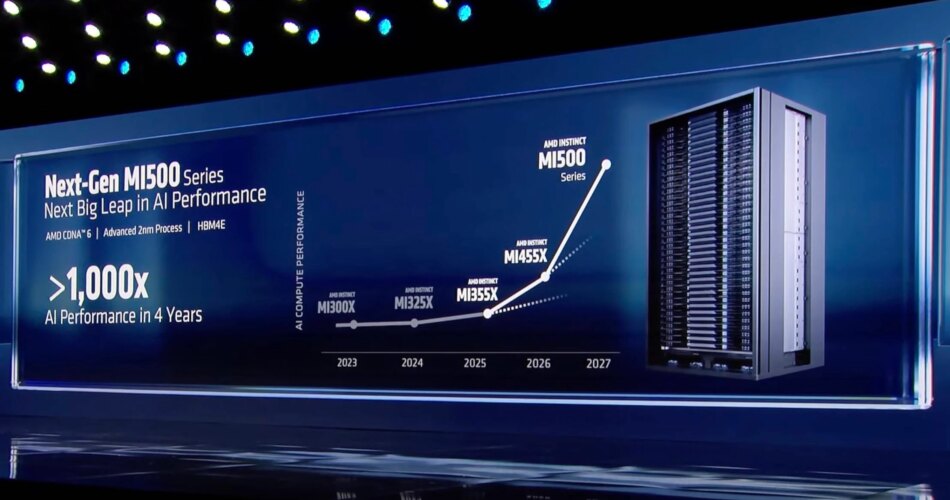
AMD teased its next-generation of AI accelerators at CES 2026, with CEO Lisa Su boasting the the MI500-series will ship a 1,000x uplift in efficiency over its two-year-old MI300X GPUs.
That sounds spectacular, however, as regular, the satan is within the particulars. In a press release that adopted Monday’s keynote, AMD clarified these estimates are based mostly on a comparability between an eight-GPU MI300X node and an MI500 rack system with an unspecified variety of GPUs. That is not precisely an apples-to-apples comparability.

In keeping with AMD its next-gen MI500X-series GPUs will ship an 1000x efficiency enhance over the now two-year-old MI300X. What that truly means? Exhausting to say – Click on to enlarge
The maths works out to eight MI300Xs which can be 1000x much less highly effective than X-number of MI500Xs. And since we all know basically nothing concerning the chip apart from that it will ship in 2027, pair TSMC’s 2nm course of tech with AMD’s CDNA 6 compute structure, and use HBM4e reminiscence, we won’t even start to estimate what that 1000x declare really means.
Calculating AI efficiency is not so simple as counting up the FLOPS. It is closely influenced by community latency, interconnect and reminiscence bandwidth, and the software program used to distribute the workloads throughout clusters. These components have an effect on LLM inference efficiency in another way than coaching or video technology. Due to this fact, larger than 1000x subsequently may imply something AMD needs it to.
Having stated that, if AMD needs to remain aggressive with Nvidia, the MI500-series might want to ship efficiency on par with if not higher than Nvidia’s Rubin Extremely Kyber racks. In keeping with Nvidia, when the 600kW systems make their debut subsequent 12 months, they’re going to ship 15 exaFLOPS of FP4 compute, 5 exaFLOPS of FP8 for coaching, 144 TB of HBM4e, and 4.6 PB/s of reminiscence bandwidth.
Breaking down the Intuition MI400-series
Particulars on the MI500 could also be razor skinny, however we’re beginning to get a greater image of what AMD’s MI400 sequence GPUs and rack programs will seem like.

AMD’s MI400 sequence GPUs will span three configurations from hyperscale and enterprise AI to blended AI and HPC – Click on to enlarge
At CES, AMD revealed MI400 can be supplied in at the least three flavors:
- MI455X — an AI-optimized GPU that’ll energy its Helios rack programs beginning later this 12 months.
- MI440X — a presumably lower-end model of the MI455 that’ll be supplied in a extra standard eight-way GPU field, like these utilized by the MI355x and MI325.
- MI430X — a mixed-use GPU designed to stability the calls for of each high-performance computing and AI, and will likely be deployed in at the least two upcoming supercomputers.
AMD joins the rack-scale race with Helios

AMD CEO strutted out a Helios compute blade complet with 4x MI455X GPUs and a Venice CPU at CES on Monday – Click on to enlarge
For the AI crowd, AMD’s MI455X-powered Helios racks are those to observe, as OpenAI, xAI, and Meta are anticipated to deploy them at scale.
Every of those accelerators promise round 40 petaFLOPS of dense FP4 inference efficiency or 20 petaFLOPS of FP8 for coaching, and 432 GB of HBM4 good for 19.6 TB/s and three.6 TB/s of interconnect bandwidth for chip-to-chip communications.
Presumably, these chips will assist greater precision datatypes generally utilized in coaching and picture fashions, however AMD has but to spill the beans on these figures.
On the very least, we now know what the chip will seem like. On stage, Su revealed the MI455X bundle, which can use 12 3D-stacked I/O and compute dies fabbed on TSMC’s 2 nm and three nm course of nodes. All will likely be fed by what to our eyes seems to be 12 36 GB HBM4 stacks.

There it’s. MI455X within the silicon. – Click on to enlarge
Helios will make use of 72 of those chips with one Epyc Venice CPU for each 4 GPUs forming a node.
Venice within the silicon
Talking of Venice, at CES we additionally bought our greatest look but at AMD’s highest-core-count Epyc ever.

The picture is not the sharpest, however we are able to simply make out what look like eight 32-core CCDs and a pair of I/O dies on the Venice CPU bundle – Click on to enlarge
The chips will likely be accessible with as much as 256 Zen 6 cores and can characteristic twice the reminiscence and GPU bandwidth in comparison with final gen. By GPU bandwidth, we assume AMD is speaking about PCIe lanes, which tells us that we’re taking a look at 128 lanes of PCIe 6.0 connectivity. To double the reminiscence bandwidth over Turin, in the meantime, we estimate AMD will want 16 channels of DDR5 8800.
To suit that many cores right into a single chip, Venice seems to make use of a brand new packaging approach with what appears to be like like eight 32-core chiplets and two I/O dies. There additionally look like eight tiny chiplets on both facet of the I/O chipsets, although it is not instantly apparent what objective they serve.
We do not know but whether or not the model of Venice Su was holding in her keynote is utilizing certainly one of AMD’s compact or frequency-optimized cores. Since at the least 2023, AMD has supplied two variations of its Zen cores: a bigger, higher-clocking model and a smaller, extra compact model that does not clock as excessive.
Whereas that may sound an terrible lot like Intel’s E-cores, each AMD’s Zen and Zen C cores use the identical microarchitecture. Intel’s E-cores use a special structure and cache structure from its P-cores. In consequence, they typically lack superior performance like AVX-512 and matrix accelerators.
The one variations between AMD’s cores is one will be packed extra densely with 16 cores per core complicated die (CCD) versus eight, working at decrease frequencies with barely much less cache per core.
If AMD can tackle the latter level, there will not be a have to differentiate between the 2 within the Zen 6 technology. We’ll simply have high-core depend SKUs that do not clock as excessive because the lower-core-count variations like they at all times have.
Alongside the “customary” Venice SKUs, AMD is as soon as once more providing an “X” variant of the half for prime efficiency computing. AMD’s X chips have traditionally featured 3D-stacked cache dies positioned beneath or on high of the CCD, boosting the L3 cache considerably. Genoa-X, AMD’s final datacenter X chip might be kitted out with greater than a terabyte of L3 in its highest-end configuration.
Sooner networking
We do not have much more data on AMD’s next-gen networking stack, however we all know that alongside the brand new CPUs and GPUs, Helios will even characteristic two new NICs from its Pensando division for rack-to-rack communications throughout the cluster.

Alongside the 12 Vulcano NICs, the Helios compute blade will even use Pensando’s Silina 400 DPU – Click on to enlarge
This consists of as much as twelve 800 Gbps Volcano NICs (three per GPU) which kind the scale-out compute cloth — what we name the backend community that enables workloads to be distributed throughout a number of nodes or on this case racks.
The programs will even characteristic Pensando’s Solina information processing unit, which is designed to dump issues like software-defined networking, storage, and safety so the CPUs and GPUs can deal with producing tokens or coaching fashions.
To sew Helios’s 72 GPUs into one nice huge accelerator, AMD is utilizing Extremely Accelerator Hyperlink (UALink) — an open various to Nvidia’s NVLink — tunneled over Ethernet.
Not less than for HPE’s implementation of the rack, Broadcom’s Tomahawk 6 will deal with switching.
There are solely so some ways to attach the chips, however at 102.4 Tbps, we estimate AMD will want 12 Tomahawk 6 ASICs unfold throughout six change blades. Earlier renderings of Helios appeared to point out 5 change blades which threw us for a little bit of a loop, however we have since realized the precise racks will characteristic six.
Giving Nvidia a run for its cash
Mixed, the Helios rack’s 72 GPUs promise to ship 2.9 exaFLOPS of dense FP4 efficiency, 1.4 exaFLOPS at FP8, 31 TB of HBM4, and 1.4 PB/s of reminiscence bandwidth. That places it in the identical ballpark and in some instances quicker than Nvidia’s newly unveiled Vera Rubin NVL72 rack programs, which we checked out earlier this week.
And when you’re not able to drop a couple of million bucks on a rack-scale system, AMD will even provide the MI440X in an eight-way configuration that, from what we have gathered, will use the identical OAM kind issue because the MI355X and MI325X. These programs will compete with Nvidia’s Rubin NVL8 containers which pair eight GPUs with an x86-based compute platform for area within the enterprise.
For all of the fervor round rackscale, AMD expects this kind issue to stay fairly widespread with enterprise clients that may’t, for one cause or one other, run their fashions within the cloud or entry them through a distant API.
Whereas we do not have all the small print simply but, it appears to be like like AMD will not simply be competing with Nvidia on AI efficiency, however on HPC perf as properly.
The MI430X will characteristic the identical load out of HBM4 because the MI455X at 432 GB and 19.6 TB/s. However the place MI455X is all about AI, the MI430X will use a special set of chiplets, giving it the pliability to run at both FP64 or FP32 for HPC, FP8 or FP4 for AI, or a mix of the 2 as is rapidly changing into the style.
Very similar to with the MI440X, AMD hasn’t disclosed the floating level perf of the MI430X, however utilizing publicly accessible data, the wafer wizards at Chips and Cheese suggest it might be north of 200 teraFLOPS.
Regardless of the chip’s precise floating level efficiency really finally ends up being, we all know it will be achieved in {hardware}. This units AMD aside from Nvidia, which is counting on emulation to spice up FP64 efficiency of its Rubin GPUs to 200 teraFLOPS.
We anticipate AMD can have extra to share on its Venice CPUs and the remainder of its MI400-series accelerators nearer to launch, which is anticipated someday within the second half of 2026. ®
Source link