AMD is one of the oldest designers of large scale microprocessors and the subject of polarizing debate among technology enthusiasts for nearly 50 years. Its story makes for a thrilling tale — filled with heroic successes, foolhardy errors, and a close shave with rack and ruin. Where other semiconductor firms have come and gone, AMD has weathered many storms and fought numerous battles, in boardrooms, courts, and stores.
In the third edition of this feature we revisit the company’s past, examine the twists and turns in the path to the present, and wonder at what lies ahead for this Silicon Valley veteran.
The rise to fame and fortune
To begin our story, we need to roll back the years and head for America and the late 1950s. Thriving after the hard years of World War II, this was the time and place to be if you wanted experience the forefront of technological innovation.
Companies such as Bell Laboratories, Texas Instruments, and Fairchild Semiconductor employed the very best engineers, and churned out numerous firsts: the bipolar junction transistor, the integrated circuit, and the MOSFET (metal oxide semiconductor field effect transistor).
These young technicians wanted to research and develop ever more exciting products, but with cautious senior managers mindful of the times when the world was fearful and unstable, frustration amongst the engineers build a desire to strike out alone.
And so, in 1968, two employees of Fairchild Semiconductor, Robert Noyce and Gordon Moore, left the company and forged their own path. N M Electronics opened its doors in that summer, to be renamed just weeks later as Integrated Electronics — Intel, for short.
Others followed suit and less than a year later, another 8 people left and together they set up their own electronics design and manufacturing company: Advanced Micro Devices (AMD, naturally).
The group was headed by Jerry Sanders, Fairchild’s former director of marketing, They began by redesigning parts from Fairchild and National Semiconductor rather than trying to compete directly with the likes of Intel, Motorola, and IBM (who spent significant sums of money on research and development of new integrated circuits).
From these humble beginnings, and headquartered in Silicon Valley, AMD offered products that boasted increased efficiency, stress tolerances, and speed within a few months. These microchips were designed to comply with US military quality standards, which proved a considerable advantage in the still-young computer industry, where reliability and production consistency varied greatly.
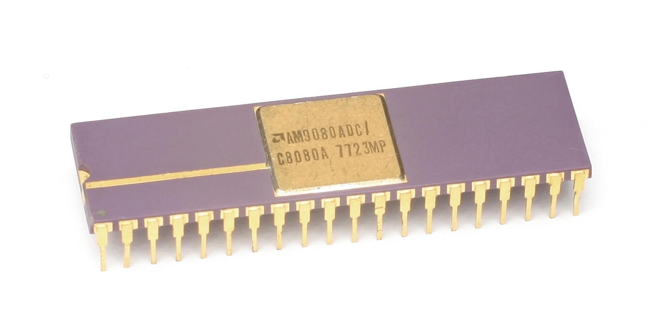
AMD’s first copycat CPU — the Am9080
By the time Intel released their first 8-bit microprocessor (the 8008) in 1974, AMD was a public company with a portfolio of over 200 products — a quarter of which were their own designs, including RAM chips, logic counters, and bit shifters. The following year saw a raft of new models: their own Am2900 integrated circuit (IC) family and the 2 MHz 8-bit Am9080, a reverse-engineered copy of Intel’s successor to the 8008. The former was a collection of components that are now fully integrated in CPUs and GPUs, but 35 years ago, arithmetic logic units and memory controllers were all separate chips.
The blatant plagiarism of Intel’s design might seem to be somewhat shocking by today’s standards, but it was par for the course in the fledgling days of microchips.
The blatant plagiarism of Intel’s design might seem to be somewhat shocking by today’s standards, but it was par for the course in the fledgling days of microchips. The CPU clone was eventually renamed as the 8080A, after AMD and Intel signed a cross-licensing agreement in 1976. You’d imagine this would cost a pretty penny or two, but it was just $325,000 ($1.65 million in today’s dollars).
The deal allowed AMD and Intel to flood the market with ridiculously profitable chips, retailing at just over $350 or twice that for ‘military’ purchases. The 8085 (3 MHz) processor followed in 1977, and was soon joined by the 8086 (8 MHz). In 1979 also saw production begin at AMD’s Austin, Texas facility.
When IBM began moving from mainframe systems into so-called personal computers (PCs) in 1982, the outfit decided to outsource parts rather than develop processors in-house. Intel’s 8086, the first ever x86 processor, was chosen with the express stipulation that AMD acted as a secondary source to guarantee a constant supply for IBM’s PC/AT.
A contract between AMD and Intel was signed in February of that year, with the former producing 8086, 8088, 80186, and 80188 processors — not just for IBM, but for the many IBM clones that proliferated (Compaq being just one of them). AMD also started manufacturing the 16-bit Intel 80286, badged as the Am286, towards the end of 1982.
This was to become the first truly significant desktop PC processor, and while Intel’s models generally ranged from 6 to 10 MHz, AMD’s started at 8 MHz and went as high as 20 MHz. This undoubtedly marked the start of the battle for CPU dominance between the two Silicon Valley powerhouses; what Intel designed, AMD simply tried to make better.
Am286, Am386… Am5x86
This period represented a huge growth of the fledgling PC market, and noting that AMD had offered the Am286 with a significant speed boost over the 80286, Intel attempted to stop AMD in its tracks. This was done by excluding them from gaining a licence for the next generation 386 processors.
AMD sued, but arbitration took four and a half years to complete, and while the judgment found that Intel was not obligated to transfer every new product to AMD, it was determined that the larger chipmaker had breached an implied covenant of good faith.
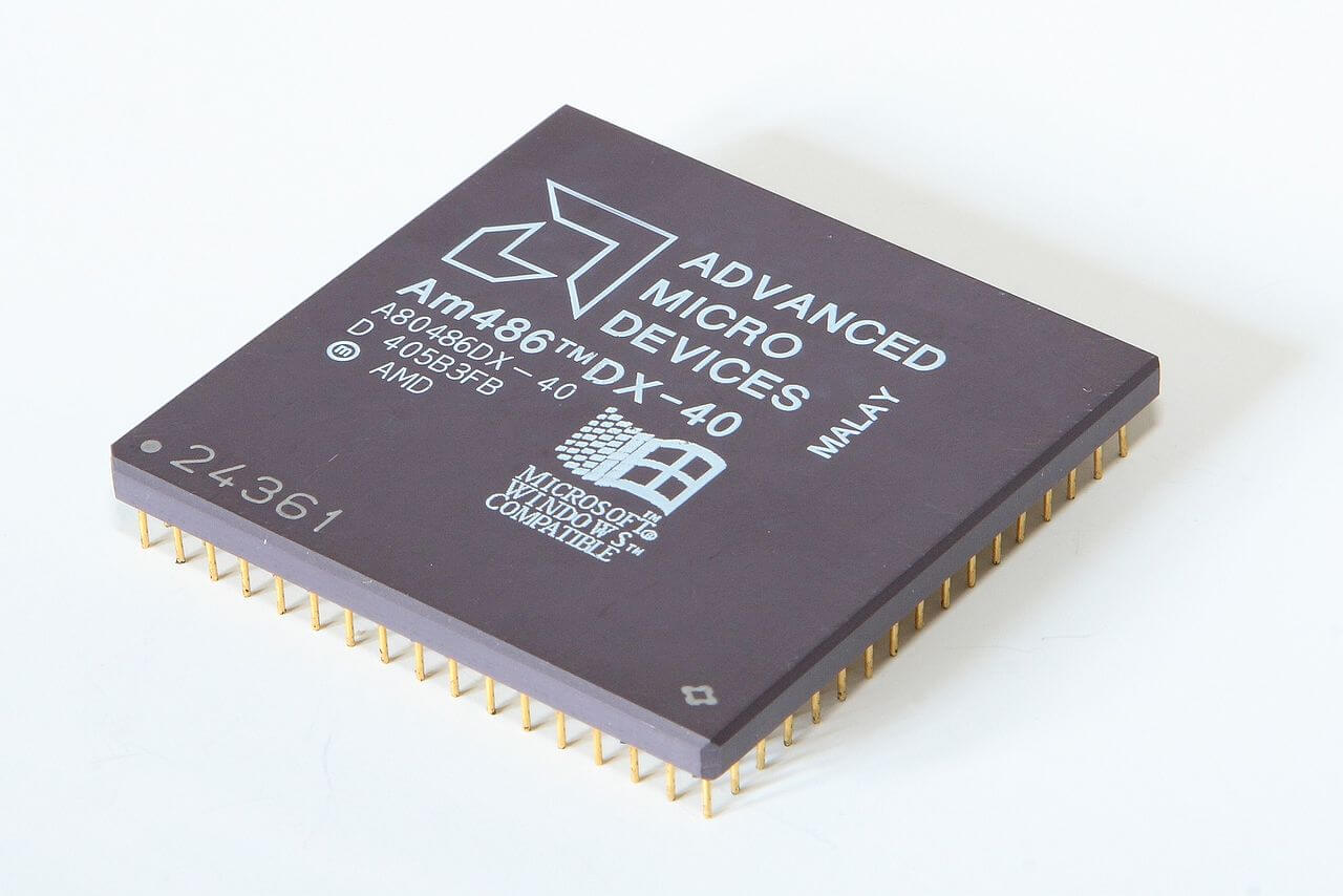
Intel’s licence denial occurred during a critical period, right as IBM PC’s market was ballooning from 55% to 84%. Left without access to new processor specifications, AMD took over five years to reverse-engineer the 80386 into the Am386. Once completed, it proved once more to be more than a match for Intel’s model. Where the original 386 debuted at just 12 MHz in 1985, and later managed to reach 33 MHz, the top-end version of the Am386DX launched in 1989 at 40 MHz.
The Am386’s success was followed by the release of 1993’s highly competitive 40 MHz Am486, which offered roughly 20% more performance than Intel’s 33 MHz i486 for the same price. This was to be replicated throughout the entire 486 line up, and while Intel’s 486DX topped out at 100 MHz, AMD offered (somewhat predictably at this stage) a snappier 120 MHz option. To better illustrate AMD’s good fortune in this period, the company’s revenue doubled from just over $1 billion in 1990 to well over $2 billion in 1994.
In 1995, AMD introduced the Am5x86 processor as a successor to the 486, offering it as a direct upgrade for older computers.
In 1995, AMD introduced the Am5x86 processor as a successor to the 486, offering it as a direct upgrade for older computers. The Am5x86 P75+ boasted a 150 Mhz frequency, with the ‘P75’ referencing performance that was similar to Intel’s Pentium 75. The ‘+’ signified that the AMD chip was slightly faster at integer math than the competition.
To counter this, Intel altered its naming conventions to distance itself from products by its rival and other vendors. The Am5x86 generated significant revenue for AMD, both from new sales and for upgrades from 486 machines. As with the Am286, 386 and 486, AMD continued to extend the market scope of the parts by offering them as embedded solutions.
March 1996 saw the introduction of its first processor, developed entirely by AMD’s own engineers: the 5k86, later renamed to the K5. The chip was designed to compete with the Intel Pentium and Cyrix 6×86, and a strong execution of the project was pivotal to AMD — the chip was expected to have a much more powerful floating point unit than Cyrix’s and about equal to the Pentium 100, while the integer performance targeted the Pentium 200.
Ultimately, it was a missed opportunity, as the project was dogged by design and manufacturing issues. These resulted in the CPU not meeting frequency and performance goals, and it arrived late to market, causing it to suffer poor sales.
AMD K6 and 3DNow! era
By this time, AMD had spent $857 million in stock on NexGen, a small fabless chip (design-only) company whose processors were made by IBM. AMD’s K5 and the developmental K6 had scaling issues at higher clock speeds (~150 MHz and above) while NexGen’s Nx686 had already demonstrated a 180 MHz core speed. After the buyout, the Nx686 became AMD’s K6 and the development of the original chip was consigned to the scrapyard.
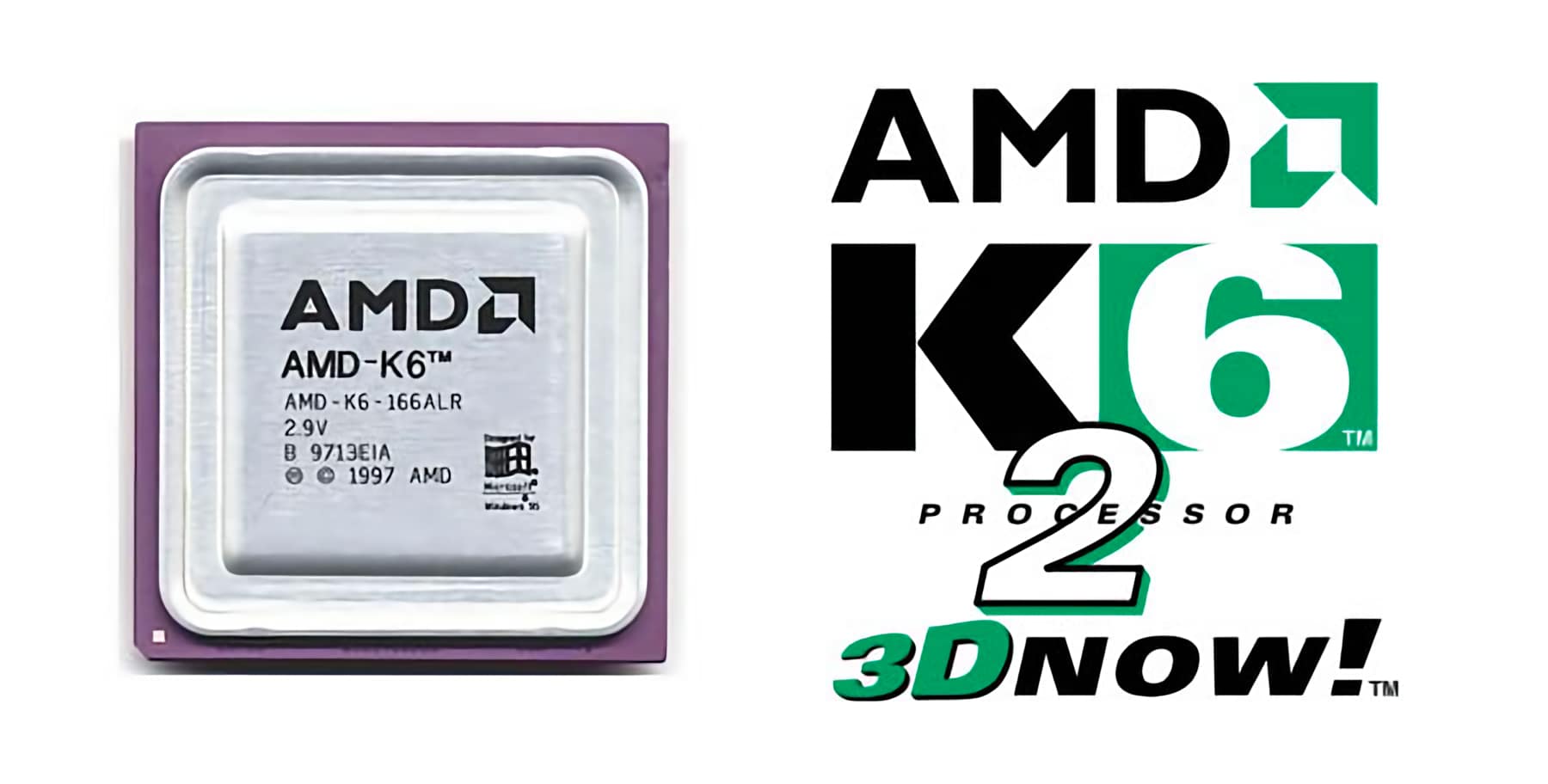
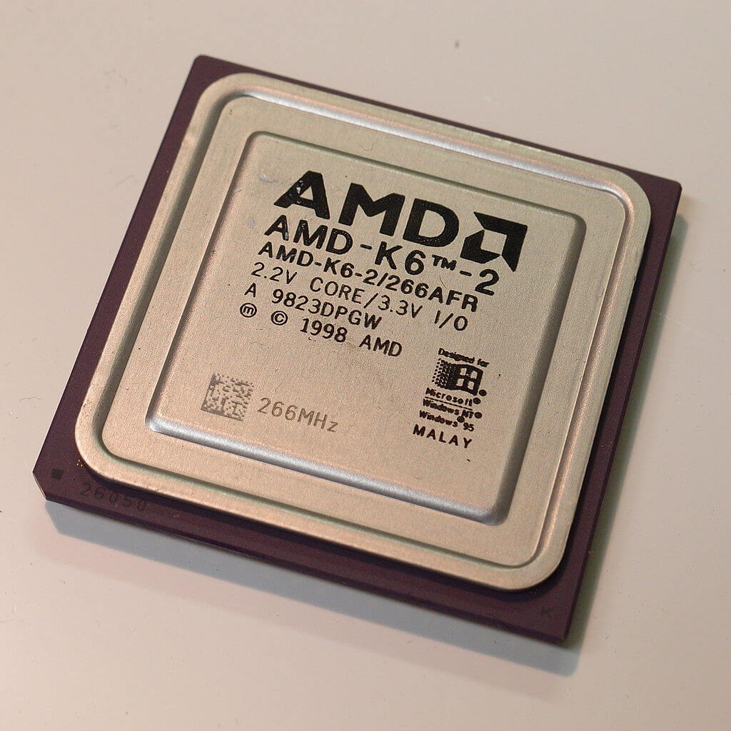
The K6-2 introduced AMD’s 3DNow! SIMD (single instruction, multiple data) instruction set.
AMD’s rise reflected Intel’s decline, from the early beginnings of the K6 architecture, which was pitted against Intel’s Pentium, Pentium II and (largely rebadged) Pentium III. The K6 produced a quickening of AMD’s success, owing its existence and capabilities to an ex-Intel employee, Vinod Dham (a.k.a. the “Father of Pentium”), who left Intel in 1995 to work at NexGen.
When the K6 hit shelves in 1997, it represented a viable alternative to the Pentium MMX. The K6 went from strength to strength — from a 233 MHz speed in the initial stepping, to 300 MHz for the “Little Foot” revision in January 1998, 350 MHz in the “Chomper” K6-2 of May 1998, and an astonishing 550 MHz in September 1998 with the “Chomper Extended” revision.
The K6-2 introduced AMD’s 3DNow! SIMD (single instruction, multiple data) instruction set. Essentially the same as Intel’s SSE, it offered an easier route accessing the CPU’s floating point capabilities; the downside to this being that programmers needed to incorporate the new instruction in any new code, in addition to patches and compilers needing to be rewritten to utilize the feature.
Like the initial K6, the K6-2 represented much better value than the competition, often costing half as much as Intel’s Pentium chips. The final iteration of the K6, the K6-III, was a more complicated CPU, and the transistor count now stood at 21.4 million — up from 8.8 million in the first K6, and 9.4 million for the K6-II.
It incorporated AMD’s PowerNow!, which dynamically altered clock speeds according to workload. With clock speeds eventually reaching 570MHz, the K6-III was fairly expensive to produce and had a relatively short life span cut short by the arrival of the K7 which was better suited to compete with the Pentium III and beyond.
First golden age: Athlon
1999 was the zenith of AMD’s golden age — the arrival of the K7 processor, branded Athlon, showed that they were truly no longer the cheap, copycat option.
Starting at 500 MHz, Athlon CPUs utilized the new Slot A (EV6) and a new internal system bus licensed from DEC that operated at 200MHz, eclipsing the 133MHz Intel offered at the time. June 2000 brought the Athlon Thunderbird, a CPU cherished by many for its overclockability, which incorporated DDR RAM support and a full speed Level 2 on-die cache.
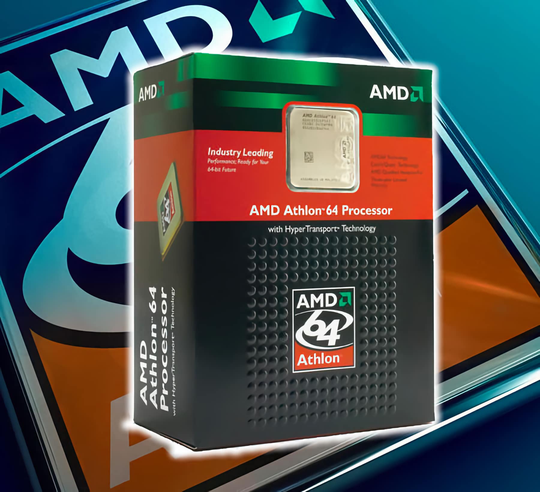
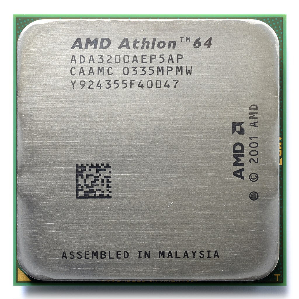
Thunderbird and its successors (Palomino, Thoroughbred, Barton, and Thorton), battled Intel’s Pentium 4 throughout the first five years of the millennium, usually at a lower price point but always with better performance. Athlon was upgraded in September 2003 with the K8 (codenamed ClawHammer), better known as the Athlon 64, because it added a 64-bit extension to the x86 instruction set.
This episode is usually cited as AMD’s defining moment. While it was surging ahead, the MHz-at-any-cost approach of Intel’s Netburst architecture was being exposed as a classic example of a developmental dead end.
Revenue and operating income were both excellent for such a relatively small company. While not achieving Intel’s levels of income, AMD was flush with success and hungry for more. But when you’re at the very peak of the tallest of mountains, it takes every ounce of effort to stay there — otherwise, there’s only way to go.
Paradise lost: AMD tumbles
There is no single event responsible for AMD tumbling from its lofty position. A global economy crisis, internal mismanagement, poor financial predictions, a victim of its own success, the fortunes and misdeeds of Intel — these all played a part, in some way or another.
But let’s start seeing how matters were in early 2006. The CPU market was satiated with offerings from both AMD and Intel, but the former had the likes of the exceptional K8-based Athlon 64 FX series. The FX-60 was a dual-core 2.6 GHz, whereas the FX-57 was single core, but ran at 2.8 GHz.
Both were head-and-shoulders above anything else, as shown by reviews at the time. They were hugely expensive, with the FX-60 retailing at over $1,000, but so was Intel’s creme-de-la-creme, the 3.46 GHz Pentium Extreme Edition 955. AMD seemed to have the upper hand in the workstation/server market as well, with Opteron chips outperforming Intel’s Xeon processors.
The problem for Intel was their Netburst architecture — the ultra-deep pipeline structure required very high clock speeds to be competitive, which in turn increased power consumption and heat output. The design had reached its limits and was no longer up to scratch, so Intel ditched its development and turned to their older Pentium Pro/Pentium M CPU architecture to build a successor for the Pentium 4.
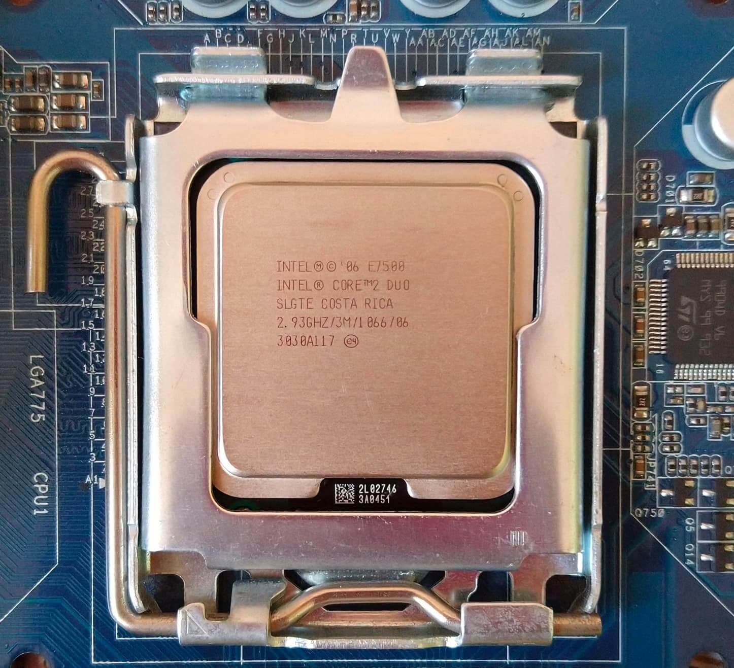
The initiative first produced the Yonah design for mobile platforms and then the dual-core Conroe architecture for desktops, in August 2006. Such was Intel’s need to save face that they relegated the Pentium name to low-end budget models and replaced it with Core — 13 years of brand dominance swept away in an instant.
The move to a low-power, high-throughput chip design wound up being ideally suited to a multitude of evolving markets and almost overnight, Intel took the performance crown in the mainstream and enthusiast sectors. By the end of 2006, AMD had been firmly pushed from the CPU summit, but it was a disastrous managerial decision that pushed them right down the slope.
Intel cores and AMD buys ATI
Three days before Intel launched the Core 2 Duo, AMD made public a move that had been fully approved by then-CEO Hector Ruiz (Sanders had retired 4 years earlier). On July 24 2006, AMD announced that it intended to acquire the graphics card manufacturer ATI Technologies, in a deal worth $5.4 billion (comprising $4.3 billion in cash and loans, and $1.1 billion raised from 58 million shares).
The deal was a huge financial gamble, representing 50% of AMD’s market capitalization at the time, and while the purchase made sense, the price absolutely did not.
Imageon, the handheld graphics division of ATI, was sold to Qualcomm in a paltry $65 million deal. That division is now named Adreno, an anagram of “Radeon” and an integral component of the Snapdragon SoC
ATI was grossly overvalued, as it wasn’t (nor was Nvidia) pulling in anything close to that kind of revenue. ATI had no manufacturing sites, either — it’s worth was almost entirely based on intellectual property.
AMD eventually acknowledged this mistake when it absorbed $2.65 billion in write-downs due to overestimating ATI’s goodwill valuation.
To compound the lack of management foresight, Imageon, the handheld graphics division of ATI, was sold to Qualcomm in a paltry $65 million deal. That division was later named Adreno, an anagram of “Radeon” and an integral component of the Snapdragon mobile SoC (!).
Xilleon, a 32-bit SoC for Digital TV and TV cable boxes, was shipped off to Broadcom for $192.8 million.
Hardware bugs: TLB
In addition to burning money, AMD’s eventual response to Intel’s refreshed architecture was distinctly underwhelming. Two weeks after Core 2’s release, AMD’s President and COO, Dirk Meyer, announced the finalization of AMD’s new K10 Barcelona processor. This would be their decisive move in the server market, as it was a fully-fledged quad core CPU, whereas at the time, Intel only produced dual core Xeon chips.
The new Opteron chip appeared in September 2007, to much fanfare, but instead of stealing Intel’s thunder, the party officially halted with the discovery of a bug that in rare circumstances could result in lockups when involving nested cache writes. Rare or not, the TLB bug put a stop to AMD’s K10 production; in the meantime, a BIOS patch that cured the problem on outgoing processors, would do so at the loss of roughly 10% performance. By the time the revised ‘B3 stepping’ CPUs shipped 6 months later, the damage had been done, both for sales and reputation.
A year later, near the end of 2007, AMD brought the quad-core K10 design to the desktop market. By then, Intel was forging ahead and had released the now-famous Core 2 Quad Q6600. On paper, the K10 was the superior design — all four cores were in the same die, unlike the Q6600 which used two separate dies on the same package. However, AMD was struggling to hit expected clock speeds, and the best version of the new CPU was just 2.3 GHz. That was slower, albeit by 100 MHz, than the Q6600, but it was also a little more expensive.
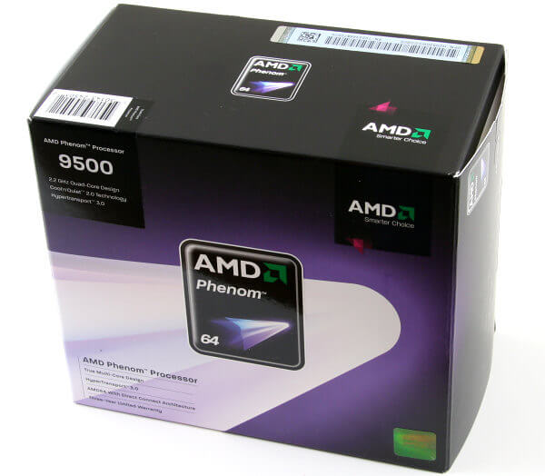
But the most puzzling aspect of it all was AMD’s decision to come out with a new model name: Phenom. Intel switched to Core because Pentium had become synonymous with excessive price and power, and having relatively poor performance. On the other hand, Athlon was a name that computing enthusiasts knew all too well and it had the speed to match its reputation. The first version of Phenom wasn’t actually bad — it just wasn’t as good as the Core 2 Quad Q6600, a product that was already readily available, plus Intel had faster offerings on the market, too.
Bizarrely, AMD seemed to make a conscious effort to abstain from advertising. They also had zero presence on the software side of the business; a very curious way to run a business, let alone one fighting in the semiconductor trade. But no review of this era in AMD’s history would be complete without taking into consideration Intel’s anti-competitive deeds. At this juncture, AMD was not only fighting Intel’s chips, but also the company’s monopolistic activities, which included paying OEMs large sums of money — billions in total — to actively keep AMD CPUs out of new computers.
In the first quarter of 2007, Intel paid Dell $723 million to remain the sole provider of its processors and chipsets — accounting for 76% of the company’s total operating income of $949 million. AMD would later win a $1.25 billion settlement in the matter, surprisingly low on the surface, but probably exacerbated by the fact that at the time of Intel’s shenanigans, AMD itself couldn’t actually supply enough CPUs to its existing customers.
Not that Intel needed to do any of this. Unlike AMD, they had rigid long-term goal setting, as well as greater product and IP diversity. They also had cash reserves like no one else: by the end of the first decade in the new millenium, Intel was pulling in over $40 billion in revenue and $15 billion in operating income. This provided huge budgets for marketing, research and software development, as well as foundries uniquely tailored to its own products and timetable. Those factors alone ensured AMD struggled for market share.
A multi-billion dollar overpayment for ATI and attendant loan interest, a disappointing successor to the K8, and problematic chips arriving late to market, were all bitter pills to swallow. But matters were about to get worse.
One step forward, one sideways, any number back
By 2010, the global economy was struggling to rebound from the financial crisis of 2008. AMD had ejected its flash memory section a few years earlier, along with all its chip making foundries — they ultimately became GlobalFoundries, which AMD still uses for some of its products. Roughly 10% of its workforce had been dropped, and all together the savings and cash injection meant that AMD could knuckle down and focus entirely on processor design.
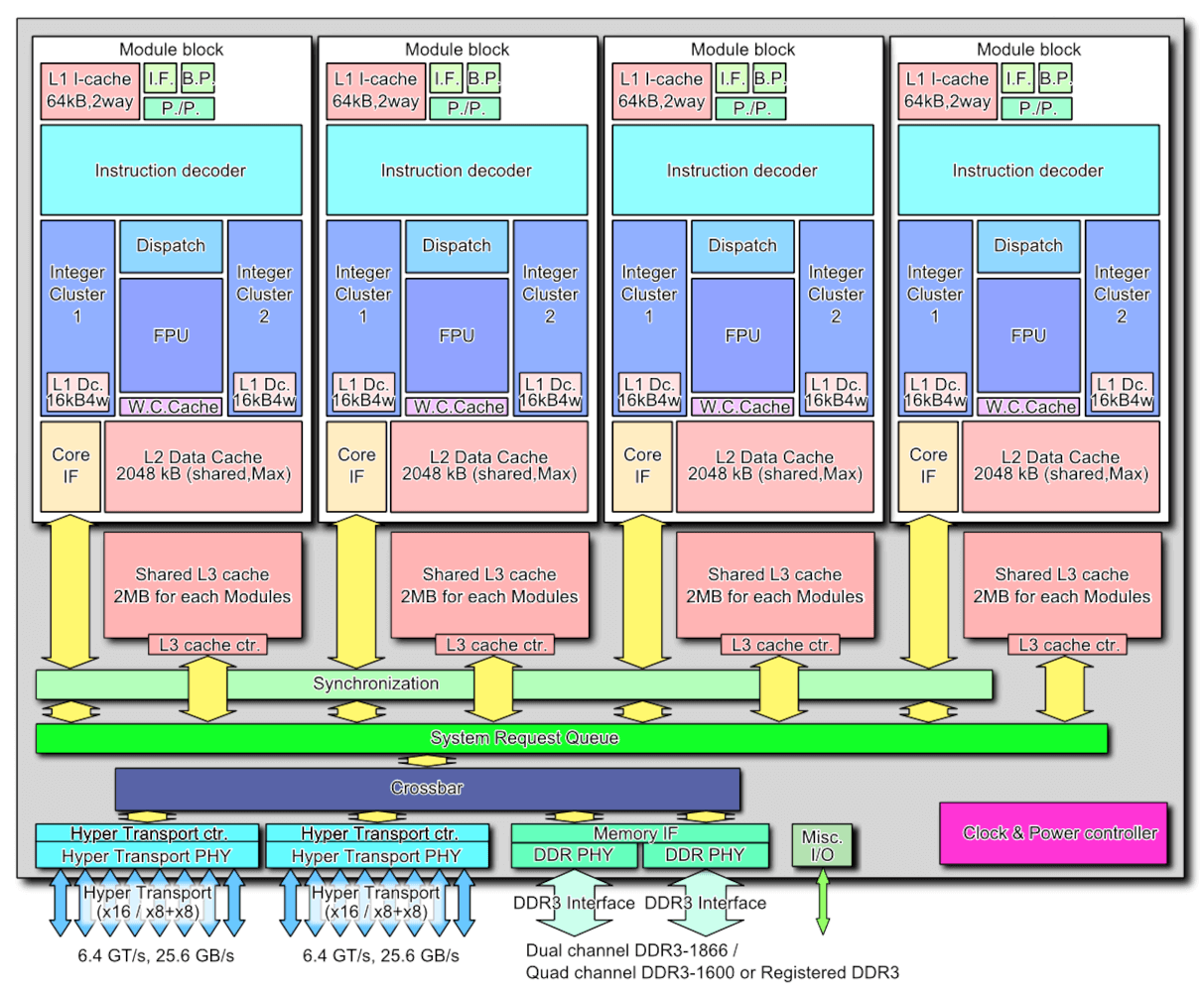
Rather than improving the K10 design, AMD started afresh with a new structure, and towards the end of 2011, the Bulldozer architecture was launched. Where K8 and K10 were true multicore, simultaneous multithreaded (SMT) processors, the new layout was classed as being ‘clustered multithreading.’
AMD took a shared, modular approach with Bulldozer — each cluster (or module) contained two integer processing cores, but they weren’t totally independent. They shared the L1 instruction and L2 data caches, the fetch/decode, and the floating point unit. AMD even went as far as to drop the Phenom name and hark back to their glory days of the Athlon FX, by simply naming the first Bulldozer CPUs as AMD FX.
The idea behind all of these changes was to reduce the overall size of the chips and make them more power efficient. Smaller dies would improve fabrication yields, leading to better margins, and the increase in efficiency would help to boost clock speeds. The scalable design would also make it suitable for a wider range of markets.
The best model in the October 2011 launch, the FX-8510, sported 4 clusters but was marketed as an 8 core, 8 thread CPU. By this era, processors had multiple clock speeds, and the FX-8150 base frequency was 3.6 GHz, with a turbo clock of 4.2 GHz. However, the chip was 315 square mm in size and had a peak power consumption of over 125 W. Intel had already released the Core i7-2600K: it was a traditional 4 core, 8 thread CPU, running at up to 3.8 GHz. It was significantly smaller than the new AMD chip, at 216 square mm, and used 30 W less power.
On paper, the new FX should have dominated, but its performance was somewhat underwhelming — at times, the ability to handle lots of threads would shine through, but single threaded performance was often no better than the Phenom range it was set to replace, despite the superior clock speeds.
Having invested millions of dollars into Bulldozer’s R&D, AMD was certainly not going to abandon the design and the purchase of ATI was now starting to bear fruit. In the previous decade, AMD’s first foray into a combined CPU and GPU package, called Fusion, was late to market and disappointingly weak.
But the project provided AMD with the means with which to tackle other markets. Earlier in 2011, another new architecture had been released, called Bobcat.
Aimed at low power applications, such as embedded systems, tablets, and notebooks; it was also the polar opposite design to Bulldozer: just a handful of pipelines and nothing much else. Bobcat received a much-needed update a few years later, into the Jaguar architecture, and was selected by Microsoft and Sony to power the Xbox One and PlayStation 4 in 2013.
Powering gaming consoles
AMD’s Bobcat received an update into the Jaguar architecture, and was selected by Microsoft and Sony to power the Xbox One and PlayStation 4 in 2013.
Although the profit margins would be relatively slim as consoles are typically built down to the lowest possible price, both platforms sold in the millions and this highlighted AMD’s ability to create custom SoCs.
AMD continued revising the Bulldozer design over the years — Piledriver came first and gave us the FX-9550 (a 220 W, 5 GHz monstrosity), but Steamroller and the final version, Excavator (launched in 2011, with products using it 4 years later), were more focused on reducing the power consumption, rather than offering anything particularly new.
By then, the naming structure for CPUs had become confusing, to say the least. Phenom was long resigned to the history books, and FX was having a somewhat poor reputation. AMD abandoned that nomenclature and just labeled their Excavator desktop CPUs as the A-series.
The graphics section of the company, fielding the Radeon products, had similarly mixed fortunes. AMD retained the ATI brand name until 2010, swapping it for their own. They also completely rewrote the GPU architecture created by ATI in late 2011, with the release of Graphics Core Next (GCN). This design would last for nearly 8 years, finding its way into consoles, desktop PCs, workstations and servers; it’s still in use today as the integrated GPU in AMD’s so-called APU processors.
GCN processors grew to have immense compute performance, but the structure wasn’t the easiest to get the best out of it. The most powerful version AMD ever made, the Vega 20 GPU in the Radeon VII, boasted 13.4 TFLOPs of processing power and 1024 GB/s of bandwidth — but in games, it just couldn’t reach the same heights as the best from Nvidia.
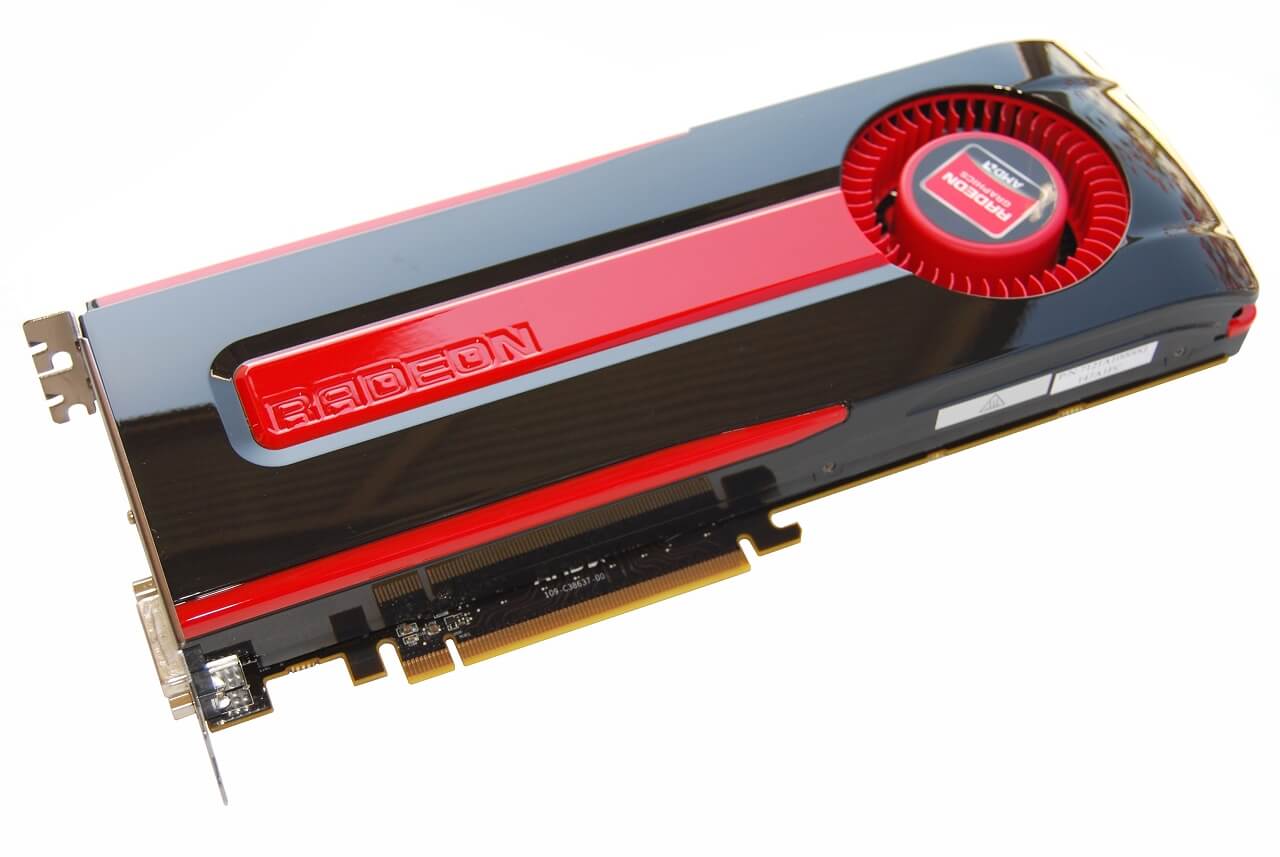
Radeon products often came with a reputation for being hot, noisy, and very power hungry. The initial iteration of GCN, powering the HD 7970, required well over 200 W of power at full load — but it was manufactured on a relatively large process node, TSMC’s 28nm. By the time GCN had reached full maturity, in the form of the Vega 10, the chips were being made by GlobalFoundries on their 14nm node, but energy requirements were no better with the likes of the Radeon RX Vega 64 consuming a maximum of nearly 300 W.
While AMD had decent product selection, they just weren’t as good as they should have been, and they struggled to earn enough money.
| Financial Year | Revenue ($ billion) | Gross Margin | Operating Income ($ million) | Net Income ($ million) |
| 2016 | 4.27 | 23% | -372 | -497 |
| 2015 | 4.00 | 27% | -481 | -660 |
| 2014 | 5.51 | 33% | -155 | -403 |
| 2013 | 5.30 | 37% | 103 | -83 |
| 2012 | 5.42 | 23% | -1060 | -1180 |
| 2011 | 6.57 | 45% | 368 | 491 |
By the end of 2016, the company’s balance sheet had taken a loss for 4 consecutive years (2012’s financials were battered by a $700 million GlobalFoundries final write off). Debt was still high, even with the sale of its foundries and other branches, and not even the success of the system package in the Xbox and PlayStation provided enough help.
At face value, AMD looked to be in deep trouble.
New stars a-Ryzen
With nothing left to sell and no sign of any large investments coming to save them, AMD could only do one thing: double-down and restructure. In 2012, they picked up two people who would come to play vital roles in the revival of the semiconductor company.
Jim Keller, the former lead architect for the K8 range, had returned after a 13 year absence and set about heading up two projects: one an Arm-based design for the server markets, the other a standard x86 architecture, with Mike Clark (lead designer of Bulldozer) being the chief architect.
Joining him was Lisa Su, who had been Senior Vice President and General Manager at Freescale Semiconductors. She took up the same position at AMD and is generally credited, along with then-President Rory Read, as being behind the company’s move into markets beyond the PC, especially consoles.
Two years after Keller’s restoration in AMD’s R&D section, CEO Rory Read stepped down and the SVP/GM moved up. With a doctorate in electronic engineering from MIT and having conducted research into SOI (silicon-on-insulator) MOSFETS, Su had the academic background and the industrial experience needed to return AMD to its glory days. But nothing happens overnight in the world of large scale processors — chip designs take several years, at best, before they are ready for market. AMD would have to ride the storm until such plans could come to fruition.
While AMD continued to struggle, Intel went from strength to strength. The Core architecture and fabrication process nodes had matured nicely, and at the end of 2016, they posted a revenue of almost $60 billion. For a number of years, Intel had been following a ‘tick-tock‘ approach to processor development: a ‘tick‘ would be a new architecture, whereas a ‘tock‘ would be a process refinement, typically in the form of a smaller node.
However, not all was well behind the scenes, despite the huge profits and near-total market dominance. In 2012, Intel expected to be releasing CPUs on a cutting-edge 10nm node within 3 years. That particular tock never happened — indeed, the clock never really ticked, either. Their first 14nm CPU, using the Broadwell architecture, appeared in 2015 and the node and fundamental design remained in place for half a decade.
The engineers at the foundries repeatedly hit yield issues with 10nm, forcing Intel to refine the older process and architecture each year. Clock speeds and power consumption climbed ever higher, but no new designs were forthcoming; an echo, perhaps, of their Netburst days. PC customers were left with frustrating choices: choose something from the powerful Core line, but pay a hefty price, or choose the weaker and cheaper FX/A-series.
But AMD had been quietly building a winning set of cards and played their hand in February 2016, at the annual E3 event. Using the eagerly awaited Doom reboot as the announcement platform, the completely new Zen architecture was revealed to the public.
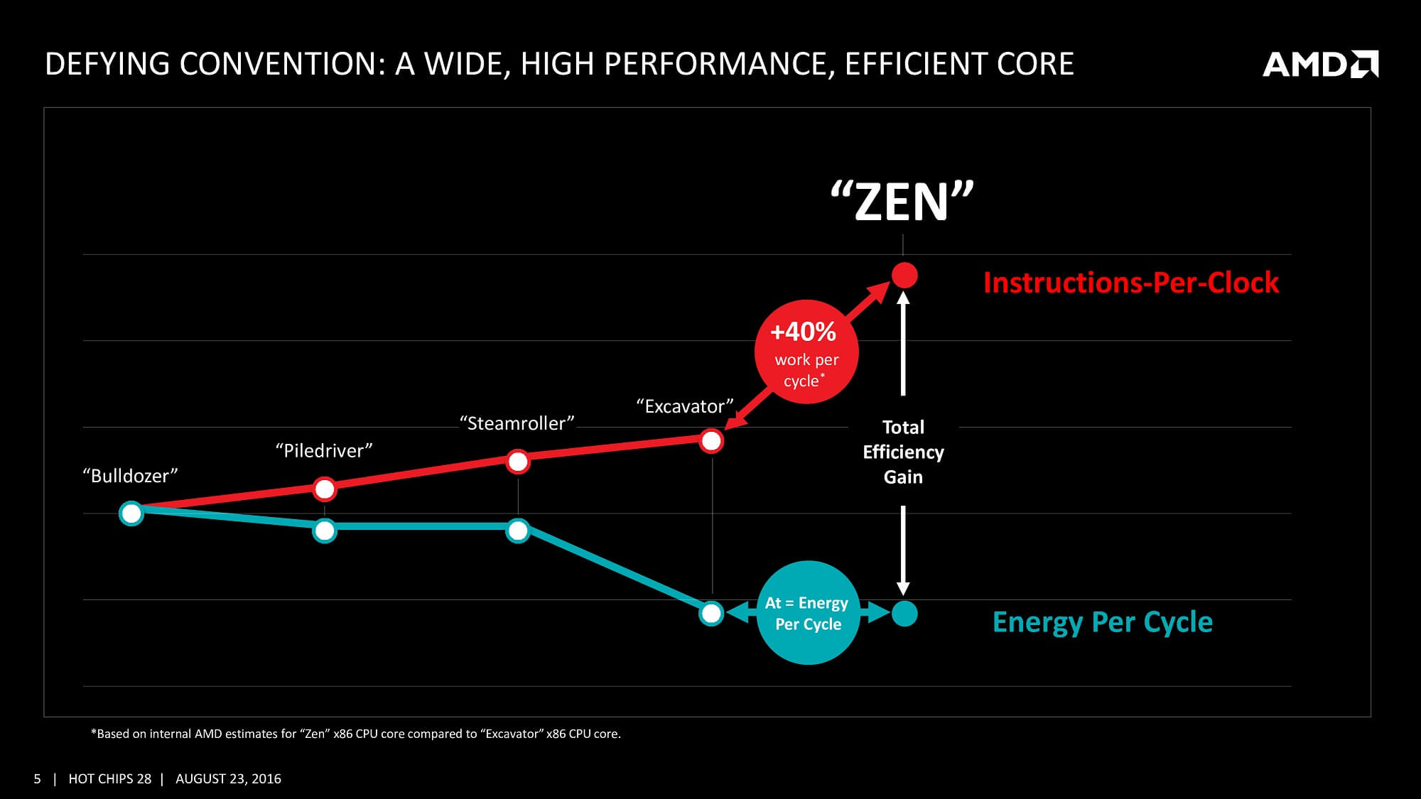
Very little was said about the fresh design besides phrases such as ‘simultaneous multithreading’, ‘high bandwidth cache,’ and ‘energy efficient finFET design.’ More details were given during Computex 2016, including a target of a 40% improvement over the Excavator architecture.
To say this was ambitious would be an understatement.
To say this was ambitious would be an understatement — especially in light of the fact that AMD had delivered modest 10% increases with each revision of the Bulldozer design, at best. It would take them another 12 months before the chip actually appeared, but when it did, AMD’s long-stewing plan was finally clear.
Any new hardware design needs the right software to sell it, but multi-threaded CPUs were facing an uphill battle. Despite consoles sporting 8-core CPUs, most games were still perfectly fine with just 4. The main reasons were Intel’s market dominance and the design of AMD’s chip in the Xbox One and PlayStation 4. The former had released their first 6-core CPU back in 2010, but it was hugely expensive (nearly $1,100). Others rapidly appeared, but it would be another seven years before Intel offered a truly affordable hexa-core processor, the Core i5-8400, at under $200.
The issue with console processors was that the CPU layout consisted of two 4-core CPUs in the same die, and there was high latency between the two sections of the chip. So game developers tended to keep the engine’s threads located on one of the sections, and only use the other for general background processes. Only in the world of workstations and servers there was a need for seriously multi-threaded CPUs — until AMD decided otherwise.
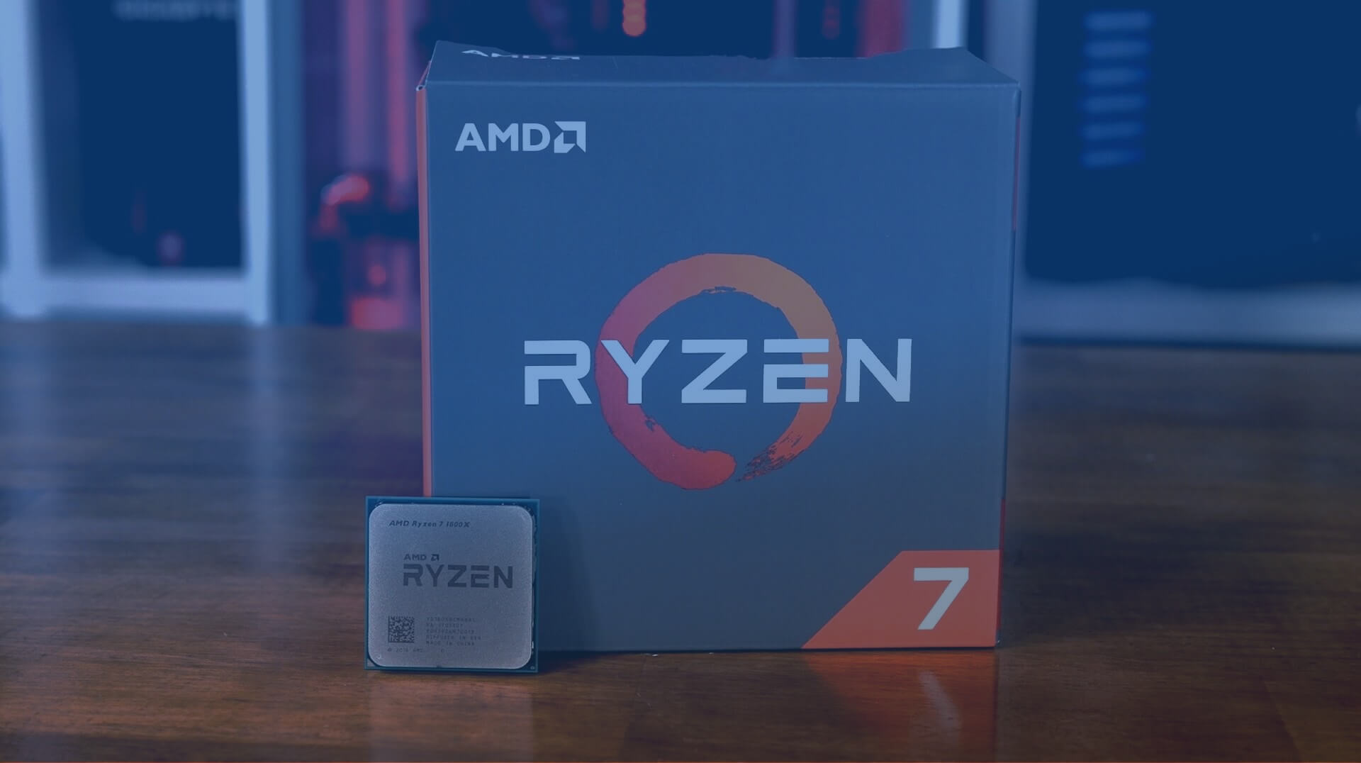
In March 2017, general desktop users could upgrade their systems with one of two 8-core,16-thread CPUs. A completely new architecture clearly deserved a new name, and AMD cast off Phenom and FX, to give us Ryzen.
Neither CPU was particularly cheap: the 3.6 GHz (4 GHz boost) Ryzen 7 1800X retailed at $500, with the 0.2 GHz slower 1700X selling for $100 less. In part, AMD was keen to stop the perception of being the budget choice, but it was mostly because Intel was charging over $1,000 for their 8-core offering, the Core i7-6900K.
Zen took the best from all previous designs and melded them into a structure that focused on keeping the pipelines as busy as possible; and to do this, required significant improvements to the pipeline and cache systems. The new design dropped the sharing of L1/L2 caches, as used in Bulldozer, and each core was now fully independent, with more pipelines, better branch prediction, and greater cache bandwidth.
Reminiscent of the chip powering Microsoft and Sony’s consoles, the Ryzen CPU was also a system-on-a-chip
Reminiscent of the chip powering Microsoft and Sony’s consoles, the Ryzen CPU was also a system-on-a-chip; the only thing it lacked was a GPU (later budget Ryzen models included a GCN processor).
The die was sectioned into two so-called CPU complexes (CCX), each of which were 4-core, 8-threads. Also packed into the die was a Southbridge processor — the CPU offered controllers and links for PCI Express, SATA, and USB. This meant motherboards, in theory, could be made without an SB but nearly all did, just to expand the number of possible device connections.
All of this would be for nothing if Ryzen couldn’t perform, and AMD had a lot to prove in this area after years of playing second fiddle to Intel. The 1800X and 1700X weren’t perfect: as good as anything Intel had for professional applications, but slower in games.
But AMD had other cards to play: a month after the first Ryzen CPUs hit the market, came 6 and 4-core Ryzen 5 models, followed two months later by 4-core Ryzen 3 chips. They performed against Intel’s offerings in the same manner as their larger brothers, but they were significantly more cost effective.
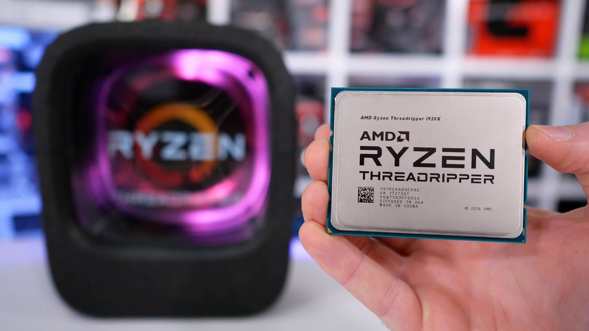
And then came the aces — the 16-core, 32-thread Ryzen Threadripper 1950X (with an asking price of $1,000) and the 32-core, 64-thread EPYC processor for servers. These behemoths comprised two and four Ryzen 7 1800X chips, respectively, in the same package, utilizing the new Infinity Fabric interconnect system to shift data between the chips.
In the space of six months, AMD showed that they were effectively targeting every x86 desktop market possible, with a single, one-size-fits-all design.
A year later, the architecture was updated to Zen+, which consisted of tweaks in the cache system and switching from GlobalFoundries’ venerable 14LPP process — a node that was under from Samsung — to an updated, denser 12LP system. The CPU dies remained the same size, but the new fabrication method allowed the processors to run at higher clock speeds.
Ryzen evolution and chiplets
AMD launched Zen 2: this time the changes were more significant and the term chiplet became all the rage
Another 12 months after that, in the summer of 2019, AMD launched Zen 2. This time the changes were more significant and the term chiplet became all the rage. Rather than following a monolithic construction, where every part of the CPU is in the same piece of silicon (which Zen and Zen+ do), the engineers separated the Core complexes from the input/output (I/O) system.
The former were manufactured by TSMC, using their N7 process, becoming full dies in their own right — hence the name, Core Complex Die (CCD). The I/O processor was fabricated by GlobalFoundries, with desktop Ryzen models using a 12LP chip, and Threadripper & EPYC sporting larger 14 nm versions.
The chiplet design was retained and refined for the next revision, Zen 3, released at the end of 2020. One major target for improvement was the CCX structure within each CCD. In Zen 2, the latter comprised two CCXs, each with 4 cores and 16MB of L3 cache.
Since L3 cache is accessible to all cores within the CPU, those from another CCX or CCD would have to request the data read and writes via the I/O die. Despite the speed and low latency of the Infinity Fabric system that connects everything together, die-to-die cache latencies weren’t great.
For Zen 3, designers kept the same overall CCD structure of 8 cores but combined them all into a single CCX. Now, the only L3 cache transactions the I/O die would have to manage were between the separate CCDs, greatly improving the data flow within each one.

With a significantly improved IPC, and multiple changes across the cache system, processor cores, and backend, the Zen architecture was maturing well. AMD’s Ryzen 5000 and 6000 series of processors, all Zen 3 chiplet or monolithic designs, proved to be immensely popular.
Some of this can be attributed to the overall value for money and performance-per-watt of the products, such as the likes of the Ryzen 5 5600X, but the main reason was the AM4 platform. First introduced with the original Zen chips, it was still supporting the new models three years later.
Not that it was all smooth sailing. AMD made a notable faux pas with the launch of the high-end 5000 series CPUs by initially stating that only motherboards with the new 500 series chipset would support them; users with older systems, such as the B350 or X470, would be out of luck. The decision was ultimately reversed, after considerable backlash from the media and enthusiast communities, but it was a timely reminder that AMD wasn’t in a position of market dominance to force such changes.
In the space of 10 years, the Zen architecture went from a blank sheet of paper to a comprehensive portfolio of products
But it’s worth taking stock of what AMD achieved with Zen. In the space of 10 years, the architecture went from a blank sheet of paper to a comprehensive portfolio of products, containing $100 6-core, 12-thread budget offerings through to $12,000+ 96-core, 192-thread server CPUs.
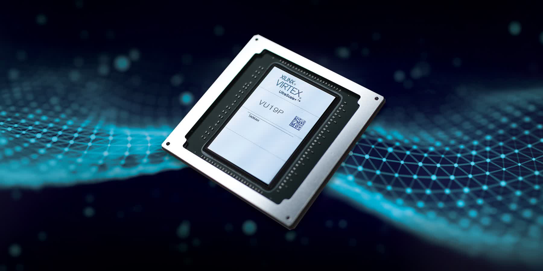
Over this time, AMD’s finances changed dramatically as well: from losses and debts running into the billions to clearing loans, posting an operating income in excess of $3.6 billion in 2021, and completing a $35 billion purchase of FPGA maker Xilinx.
While Zen may not be the sole factor in the company’s financial renaissance, it helped enormously.
AMD’s graphics division has seen similar changes in fortune — in 2015 it was given full independence, as the Radeon Technologies Group (RTG). The most significant development from their engineers came in the form of RDNA, a significant reworking of GCN. Changes to the cache structure, along with adjustments to the size and grouping of the compute units, shifted the focus of the architecture directly toward gaming.
The first line of models to use this new architecture, the Radeon RX 5700 series, appeared mid-2019 and demonstrated the design’s serious potential. This was not lost on Microsoft and Sony, as they both selected Zen 2 and the forthcoming updated RDNA 2, to power their Xbox Series X/S and PlayStation 5 consoles.
Both Microsoft and Sony selected Zen 2 and the forthcoming updated RDNA 2 to power their Xbox Series and PlayStation 5 consoles
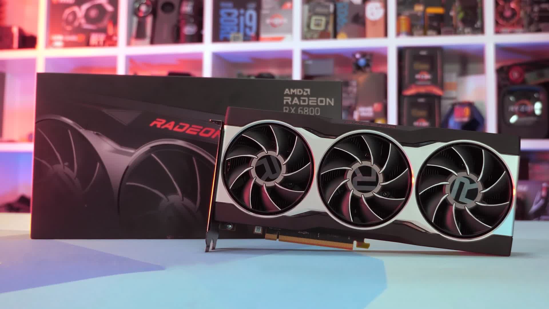
Just 14 months after the launch of the RX 5000 series, and during economic and manufacturing challenges, AMD released another Radeon lineup, with technologies from the Zen architecture featured in the new GPUs. RDNA 2 sported huge amounts of Level 3 cache, up to 128MB in total, based on the same design used in server CPUs, as well as a modified version of their Infinity Fabric interconnect system.
RTG also introduced a unique design for hardware acceleration of some of the elements of ray tracing and while Radeon RX 6000 graphics cards didn’t perform as well in this type of rendering compared to Nvidia, the overall performance was exceptionally good.
Although the Radeon Group hasn’t enjoyed the same level of financial success as the CPU division, and their graphics cards are perhaps still seen as the “value option” at times, AMD is quantifiably back to where it was in the Athlon 64 days in terms of architecture development and technological innovation. They rose to the top, fell from grace, and like a beast from mythology, created their own rebirth from the ashes
The road ahead
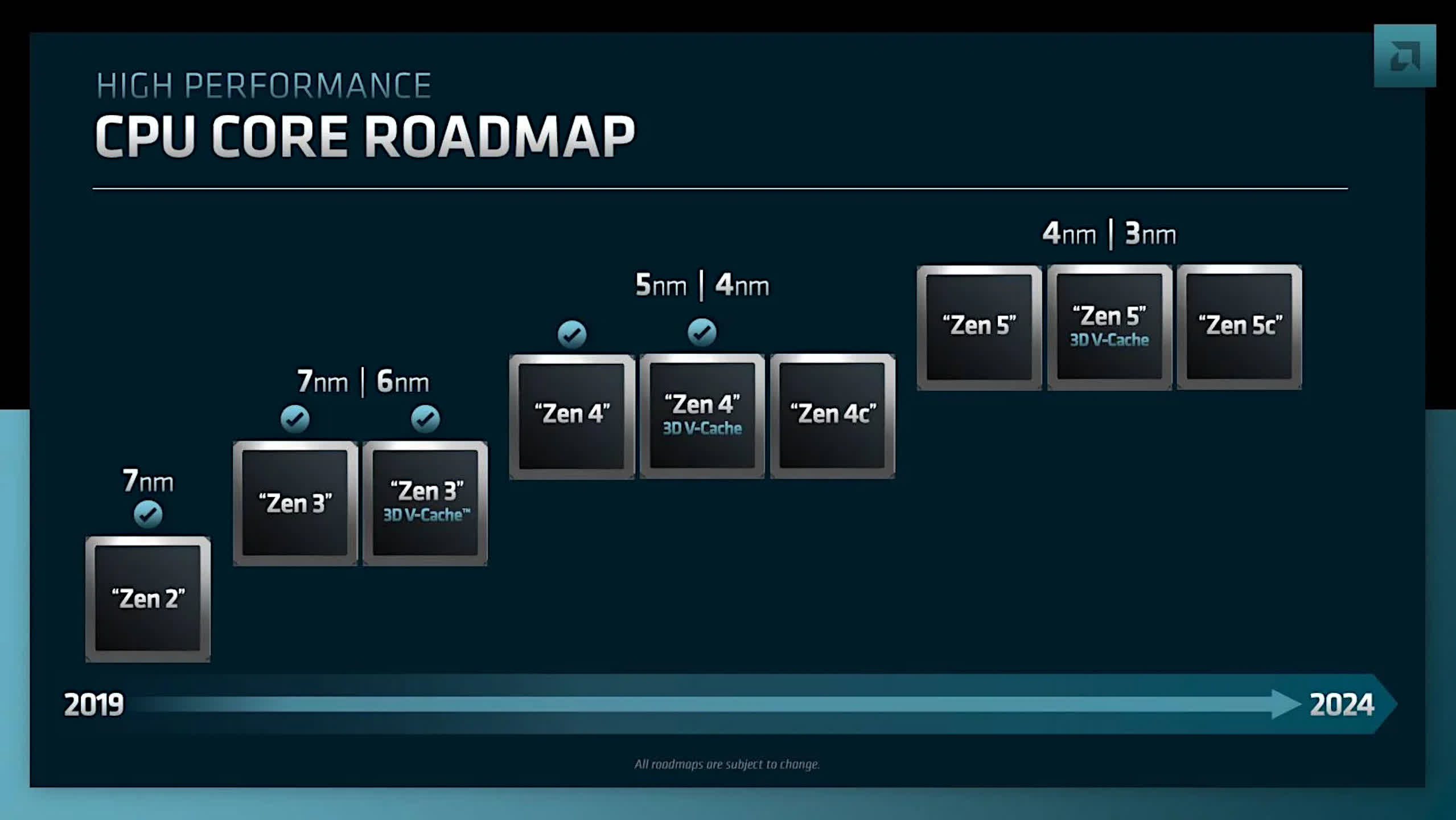
In the days of the Bulldozer architecture, AMD was playing a very conservative game, despite the somewhat radical nature of the design. That’s not a criticism that could be said of the company now. Its short-term roadmap for CPUs demonstrates this clearly…
The introduction of vertically stacked cache dies (aka 3D V-Cache) in the Ryzen 7 5800X3D was highly beneficial for gaming and is set to appear again and again. AMD’s progress with chiplets and high-speed interconnect systems made its way into graphics cards with RDNA 3, and will probably become the standard method of large GPU manufacturing in the near future.
Servers and workstations can be fitted with single processors housing more cores and cache (up to 96 and 384MB with the EPYC 9654) than ever before, and even budget desktop PCs can be found sporting 6 core processors.
All the advances made in CPU technology and parallel processing performance by AMD unquestionably forced Intel to accelerate its own heterogeneous computing designs, and the consumer is somewhat spoiled for choice now, when it comes to choosing a new processor.
To all intents and purposes, AMD appears to be as strong as any of its competitors. And yet, it’s perfectly reasonable to ask a simple question: could it return to the dark days of dismal products and no money?
A brief look at the most recent financial statements suggests that this is a possibility, but not necessarily with a high chance.
| Financial Year | Revenue ($ billion) | Net Income ($ billion) |
| 2017 | 5.33 | 0.04 |
| 2018 | 6.48 | 0.34 |
| 2019 | 6.73 | 0.34 |
| 2020 | 9.76 | 2.49 |
| 2021 | 16.4 | 3.16 |
| 2022 Q1-3 | 18.0 | 1.30 |
2021 was AMD’s best-ever year for revenue and net income, with a 19% margin. 2022 has already beaten that in terms of revenue, with the final quarter still to go, though net income will be lower.
Two new architectures, for CPUs and GPUs, were introduced in 2022 — Zen 4 brought in a raft of changes (DDR5 memory only, new AM5 platform, integrated GPU) and the new 7000 series of desktop CPUs sporting the freshly designed chips demonstrated that AMD’s engineers were showing no signs of reaching any architectural limits.
The timing of the launch couldn’t have been worse, though this was entirely unavoidable. Semiconductor manufacturing supply chains were still struggling to meet demands and with global prices rising everywhere, the high prices for DDR5 and AM5 motherboards meant that initial sales weren’t as strong as they were for Zen 3.
And despite the success of 2021, $16.4 billion of revenue still puts them behind Nvidia ($26.9 billion for roughly the same period) and light years away from Intel ($79 billion). The latter has a much larger product portfolio, of course, and its own foundries, but Nvidia’s income is reliant almost entirely on graphics processors.
It’s also worth noting that Qualcomm, another fabless processor company, experienced $33.6 billion of revenue, while IBM took in $57.4 billion, although the latter does operate in multiple different sectors.
A handful of years of healthy net income just isn’t enough to fully stabilize AMD’s future, and it’s obvious that in order to grow, revenue will need to be taken from Intel and Nvidia, as well as expanding into new markets.
The bulk of AMD’s income is from what they call the Computing and Graphics segment, i.e. Ryzen and Radeon sales. This will undoubtedly continue to improve, as Ryzen is fully competitive and the RDNA 2 and 3 architectures will provide a common platform for games that work as well on PCs as they do on consoles, given that AMD powers the current and previous generations of hardware.
Purchasing Xilinx will provide them with new markets, as the renowned FPGA company holds a bigger portion of that sector compared to Intel, as well as offer new IPs that can be integrated into current designs for new products.In previous years, AMD’s Enterprise, Embedded and Semi-Custom (EESC) segment was rather weak but has improved substantially — from just under 20% of the Q1 2020 revenue to 43% last year.
But there are still significant challenges lying in their path.
While Intel no longer dominates the desktop market in terms of outright performance, they still hold the largest portion of the market share in all sectors, especially in the enterprise industry. Nobody running a multi-million dollar data center is going to throw it all out, just because an amazing new CPU is available, no matter how good it is. And Intel now competes in the graphics card industry, too, albeit with muted success.
That sector continues to be heavily under the grasp of Nvidia, with its immensely powerful AD102 seriously raising the GPU performance bar. And while it has heavily increased prices for its new GPUs, and suffered a dip in sales accordingly, there will always be consumers who will always view cheaper products in a negative light, no matter how good they actually are.
The PlayStation 5 and Xbox Series X/S have all been very popular, with an estimated combined shipping total of over 40 million units — each one sporting an AMD unified processor. The sale of these chips played no small part in the growth of the EESC’s revenue.
However, while AMD can make a healthy profit on their EPYC server processors, Microsoft and Sony sell consoles at a loss, recouping the money via licensing fees for games. Thus, the margins for the chips in those machines will be much smaller.
It could also be argued that AMD still has an issue regarding its perceived image. The ‘Intel Inside’ catchphrase and jingle have been ubiquitous for over 30 years, and while AMD clearly spends money promoting Ryzen and Radeon brand names, they ultimately need system makers such as Dell, HP, and Lenovo to sell more units sporting their processors in the same light and specifications, as they do with Intel’s.
Where the cryptocurrency boom and demand for computing devices during the Covid pandemic did wonders for Nvidia’s share price and market capitalization (currently at an astonishing $428 billion), AMD shareholders have received more unstated gains.
That all said, AMD is currently in the strongest position that it’s ever been in 51 years. Its market cap is currently just 5% lower than Intel’s and while declining PC sales have affected almost all semiconductor share prices, AMD is weathering this storm somewhat better than Intel is.
With the ambitious Zen project showing no signs of hitting any limits soon, the company’s Phoenix-like rebirth has been a tremendous success, by any measure. They’re not at the top of the mountain yet but perhaps that’s for the better — meteoric rises are never sustainable, as we’ve seen.
It’s said that history always repeats itself, but let’s hope that this doesn’t come to pass. A healthy and competitive AMD, fully able to meet Intel and Nvidia head-on, only brings benefits to users and investors alike.
What are your thoughts on AMD and its trials and tribulations — did you own a K6 chip, or perhaps an Athlon? What’s your favorite Radeon graphics card? Which Zen-based processor are you most impressed by? Share your stories and comments in the section below.
Source link


