Intel CEO Pat Gelsinger just a few days ago raged against Bitcoin, calling it a “climate crisis.”
“A single ledger entry in Bitcoin consumes enough energy to power your house for almost a day. That’s a climate crisis. That’s not okay,” he told Bloomberg in an interview last week.
He was clearly hitting out at power-guzzling GPUs and similar chips necessary for Bitcoin mining, which requires country-size amounts of electricity as the US House Committee on Energy and Commerce heard last month.
But in under a minute in that same interview, Gelsinger – who is trying to foster an all-American farm boy at heart reputation, building in the “Silicon Heartland” in Ohio – abruptly changed his world-savior tone.
“Intel’s bringing forward a blockchain chip that’s dramatically better,” he said.
That chip, dubbed Bonanza Mine, was detailed this month at the International Solid-State Circuits Conference. This 7nm-node ASIC tries its best to minimize power consumption without cutting back on processing oomph in order to provide some degree of profitability for miners.
Bitcoin uses a blockchain to enable peer-to-peer transactions without the need of a central clearing house. Instead, the transactions are verified by validators, who are rewarded for solving complex computational problems known as proof of work that’s part of this verification process, said Vikram Suresh, a research scientist at Intel, in an online presentation. A transaction is added to Bitcoin’s distributed ledger once it has been validated. Validators are known as miners.
The proof-of-work element involves the SHA-256 cryptographic hash function, and all validators need to run this algorithm – and they need to run it fast, and a lot, to be effective miners.
Better by design?
Bonanza Mine, previewed earlier this month, includes optimizations at various levels to improve energy efficiency of hash computations.
“This includes micro architecture optimizations, optimizations in the data path arithmetic circuits, and normal latch-based clocking scheme,” Suresh said, adding “at the board level, we have die-voltage stacking. Each of these techniques offer improvement in ASIC performance, area and energy efficiency.”
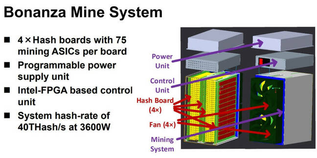
Intel has not only come up with this accelerator chip, but also created a Bitcoin mining system consisting of four circuit boards, each with 75 Bonanza Mine ASICs, adding up to a total of 300 ASICs in the system. It also has a programmable power supply, an Intel FPGA-based system controller, and four fans to cool the system.
The machine achieves a hash rate of about 40 terahashes per second while consuming 3.6kW. The system controller uses an Intel FPGA with a mining daemon running on a hard Arm Cortex core. The system uses UART serial and I2C to orchestrate the hardware.
The Bitcoin network is currently running at 188.29 exahashes per second. A high-end Antminer S19 Pro claims 110 terahashes per second with 3.25kW. An AvalonMiner A1166 Pro claims 81 TH/s in 3.4kW. You can compare Intel’s specs to the rest of the market here. Intel said its mining machine compares favorably to the Bitfury Clarke and Canaan Avalon A9.
We’ll leave it to you to decide how much or how little Intel’s chip contributes to Gelsinger’s climate crisis.
Each Bonanza Mine ASIC consists of 258 SHA-256 double-hash mining engines, which occupies 95 per cent of the die area. The ASIC also includes a controller core, sensors, and GPIO. Communication to ASICs is handled using daisy chained UART links. Bonanza Mine has a varying voltage and frequency system to balance performance and power consumption.
“Variable operating mode provides the opportunity for a miner to trade off hash rate and energy efficiency to optimize for mining profit,” Suresh said.
It has the power
One slide showed throughput and energy efficiency measurements at 75 degrees Celsius at a per-chip operating voltage of 355mV. Each ASIC can achieve a throughput of 137 gigahashes per second, requiring 55 Joules per terahash.
“The Bonanza mine system software identifies outlier engines in each ASIC and deactivates them. This helps to run the remaining engines at the highest possible frequency to optimize the overall hash rate,” Suresh said.
The mining system can be configured in three operating modes: high performance mode, a balanced mode, and a power saving mode. Depending on the mode of operation, the measured throughput ranges from 34.5 to 47.7 terahashes per second, with mining efficiency varying between 54 to 60 joules per terahash.
Suresh also talked about a three-phase latch based clocking technique that resulted in 50 per cent lower clock power.
Intel will ship the accelerator hardware direct to large cryptocurrency miners; Argo Blockchain, BLOCK (formerly known as Square), and GRIID Infrastructure. But with the wonders of capitalism, it wouldn’t be surprising if scalpers out of luck with GPUs go looking for these ASICs, which won’t be available on the open market.
Intel’s experimental chip may be an early unit to supply an emerging market focused on decentralized computing, also called Web 3.0. We imagine this will involve the exchange of cryptocurrency and digital assets in a parallel virtual universe also known as the metaverse.
Hardware and chip companies are still trying to figure out the underlying hardware that will provide this graphics-driven universe, which will need massive amounts of computing power and energy. Facebook has bet its future on the scheme, however, and Microsoft is factoring the metaverse into its future by buying Activision Blizzard for $68.7bn.
Gelsinger has promised a “Groveian” and laser-focused return of Intel to its engineering roots, while avoiding distractions on low-hanging fruit, like a past disaster called smartphones. Bitcoin is a hot market, and Intel is dabbling with it on a limited basis, though whether miners will like the new kit remains to be seen. ®


