China is reportedly planning a new chip consortium dedicated to semiconductor research and development. The new project, dubbed the “cross-border semiconductor work committee,” will launch this year. It’s to be coordinated by a lab at Tsinghua University, President Xi Jinping’s alma mater.
According to Nikkei, “the role of the committee will be to strengthen cooperation between the Chinese and foreign semiconductor industries.” That’s to be expected. China’s number one import is semiconductors and the country depends on importing chips it can’t manufacture within mainland China.
Huawei’s presence on the Entity List doesn’t prevent other Chinese companies from working with Western firms. Both Intel and AMD also have extensive business ties in China. The US government, however, may have a closer eye on these arrangements than in the past. Tech companies may also be more reticent to sign technology-sharing deals with Chinese firms. The Nikkei story doesn’t use the term “coopetition”, but the organization it describes appears intended to both partner with companies like AMD and Intel and facilitate competition with them in the long term.
The EUV Angle
There have been multiple high-profile cases of alleged IP theft between companies like Boeing, Samsung and Micron and their Chinese counterparts over the past several years. Multiple Chinese firms, including the mainland foundry SMIC, cannot purchase advanced lithography tools from companies like ASML.
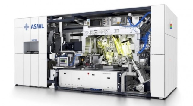
EUV (Extreme Ultraviolet Lithography) is a fundamentally new lithography technology now rolling out at the most advanced semiconductor process nodes. TSMC and Samsung have both deployed EUV in their latest nodes. Intel intends to begin transitioning to the new manufacturing technology in late 2022 with deployment in 2023. SMIC cannot take this step if it can’t buy equipment.
China’s ability to buy EUV hardware is instrumental to any effort towards semiconductor manufacturing independence. EUV replaces DUV (Deep Ultraviolet Lithography) and is less efficient and more difficult to use by virtually any metric one cares to name. EUV systems require far more power, more water for cooling, and more stringent cleanroom standards. Manufacturers have spent years developing EUV-compatible pellicles and other associated technology.
Without access to the advanced chip manufacturing hardware built by companies like ASML, companies like SMIC won’t be able to move to next-generation nodes much below 14nm. Even the equivalent of nodes like 7nm may require a steep learning curve.
When conventional dry lithography began to run out of gas around 65nm, manufacturers like TSMC and Intel introduced immersion lithography and multi-patterning to reduce minimum feature sizes below what they could achieve otherwise. Eventually, companies introduced quad-patterning. The more mask layers in a design, the greater the chance of mask misalignment or another error.
Without EUV manufacturing equipment, China has no path to advanced manufacturing nodes.
Other Technology Improvements
There are other ways that China could improve its semiconductor manufacturing without moving to new nodes. Packaging and material manufacturing changes do not require new semiconductor lithography. These improvements can deliver substantial gains on their own over time. But while lithography is not as important as it once was, the density, power, and performance improvements from moving to a smaller node are still large enough to matter over several generations.
Semiconductor manufacturing is as important to the 21st century as oil exploration was to the 20th. Most of the world’s most advanced chips are built in Taiwan, and China still claims Taiwan is a renegade province. The Taiwanese population generally takes a different view on that topic. Intel’s Pat Gelsinger has pushed the US to make a massive investment in chip manufacturing, though that issue is still being debated in Congress. As odd as it sounds, the combined performance, power, and area advantages of, say, a future 3nm node built with EUV and GAAFETs or nanowires is now a matter of national security.
China currently hopes to manufacture up to 70 percent of its domestic silicon by 2025. While it is unlikely to meet that goal, any effort to build a domestic silicon manufacturing base that can meet demand will require access to cutting edge nodes.
Now Read:
Source link


