

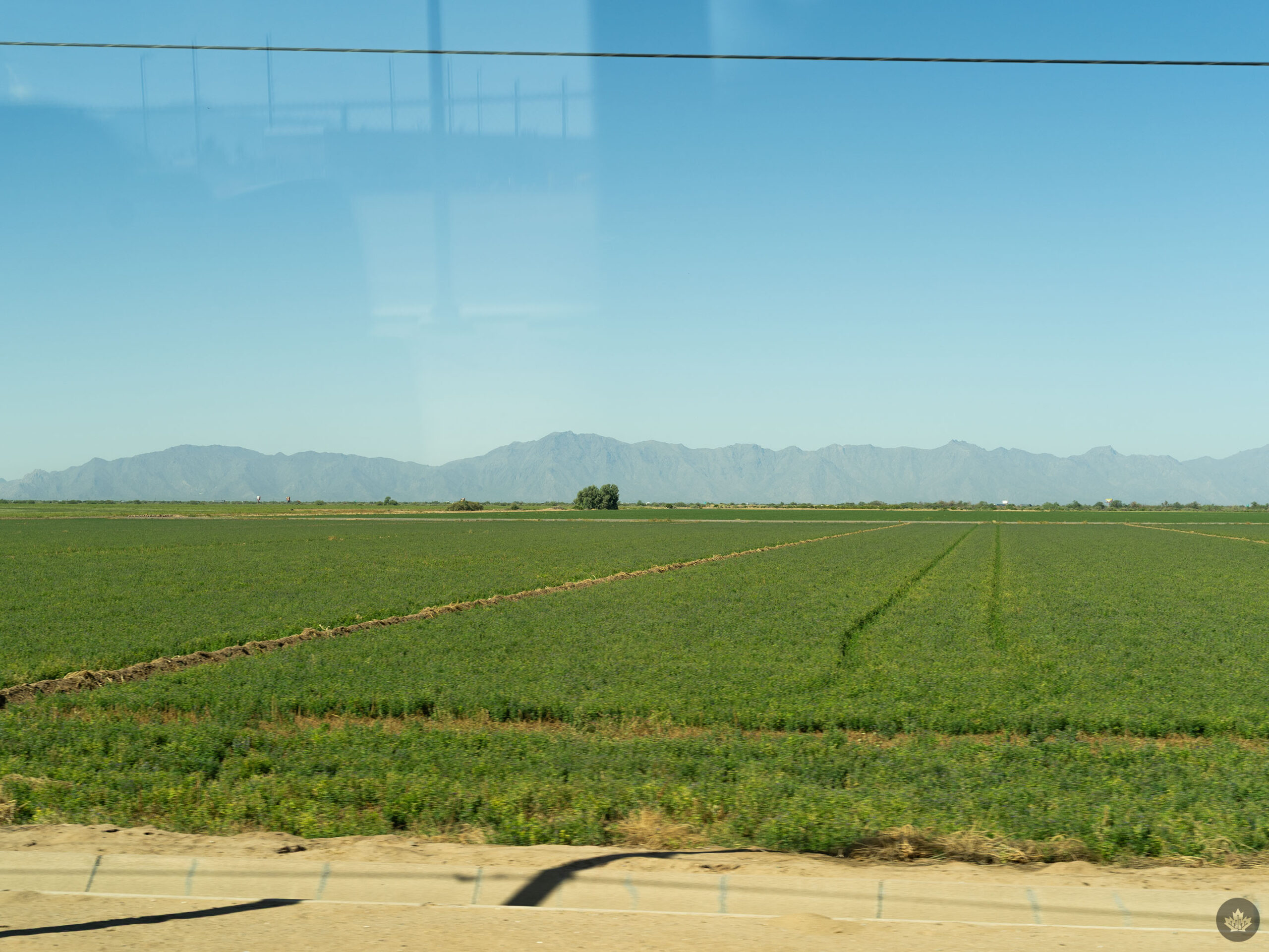
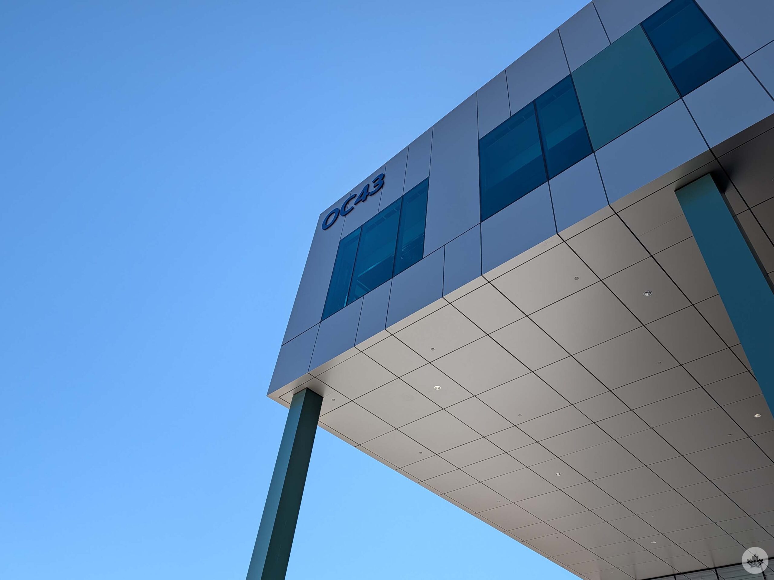
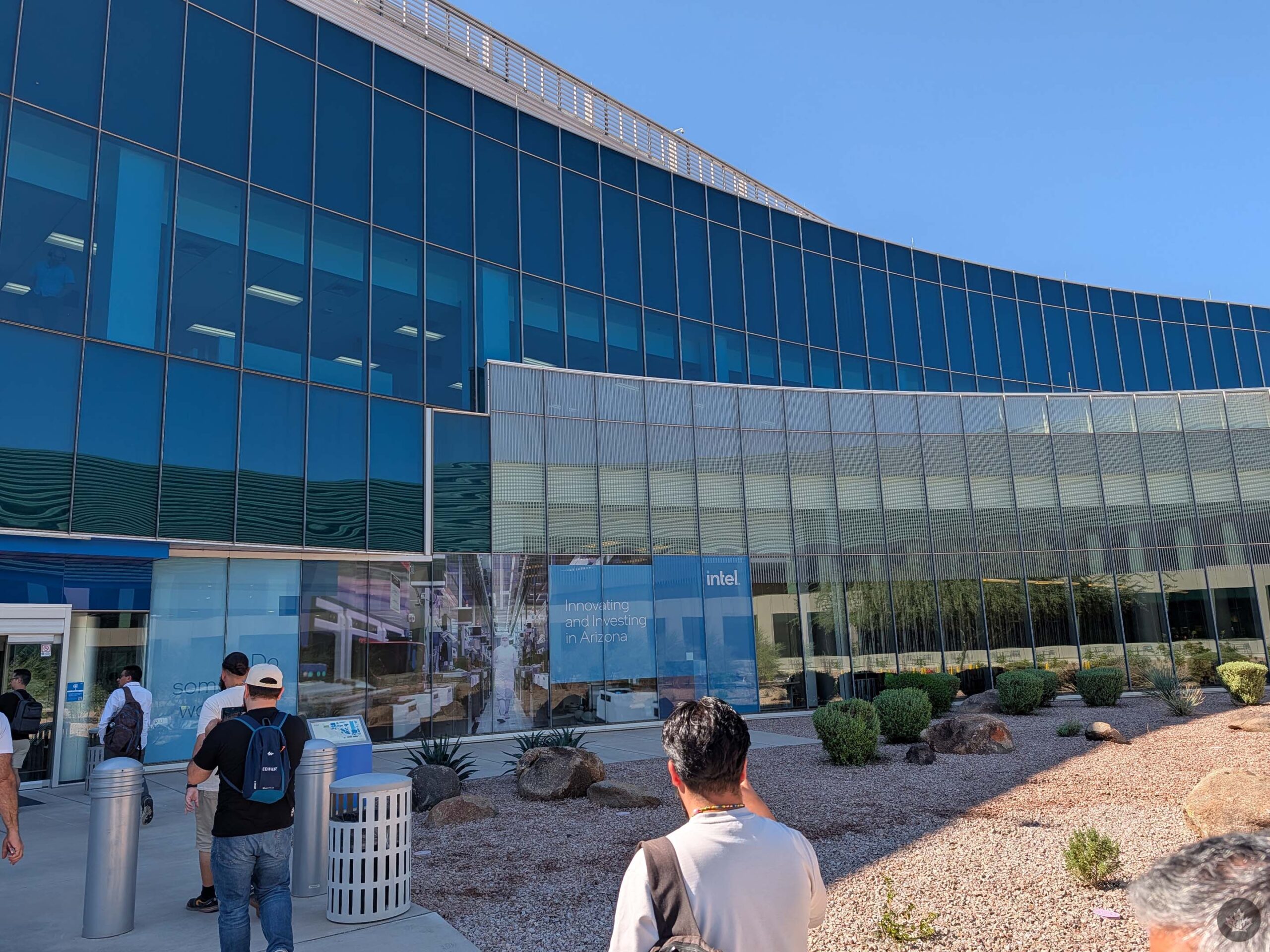
Outdated Worth Highway cuts a stark divide by way of the Arizona desert on its practically straight north-south run. West, inexperienced fields give technique to beige sand. Past, the Sierra Estrella mountains dominate the practically flat panorama. On the opposite aspect of the highway, a community of pipes connects a sequence of large buildings, giving the whole lot a vaguely steampunk vibe. That is Intel’s Ocotillo web site in Chandler, Arizona, residence of a few of the firm’s chip fabrication amenities — referred to as fabs — together with one the place the corporate makes its new Panther Lake chips.
As a part of my time at Intel’s 2025 Tech Tour in Arizona earlier this month, I received to tour the Ocotillo web site and enterprise into the brand new Fab 52 for an inside take a look at chip fabrication. The tour started with a loop across the firm’s Arizona campus, which is simply over one sq. mile in dimension and comprises a number of fabrication websites. All the campus roads sport chip-related names like Silicon Road, Processor Parkway, and Transistor Terrace.
A view of the Sierra Estrella from Intel’s Ocotillo campus.
The campus additionally options tons of coated parking — a blessing in the summertime when temperatures soar as excessive as 45°C. However extra than simply protecting the vehicles, it’s additionally photo voltaic panels. The power Intel captures this fashion is given again to the town of Chandler.
This isn’t Intel’s solely sustainability effort in Arizona. One other a part of the campus we noticed was the on-site water remedy and recycling amenities, in addition to the Ocotillo Brine Discount Facility (OBRF). The OBRF removes salt from the water earlier than additional remedy, and the eliminated salt could be reused — Intel sells it to different firms.
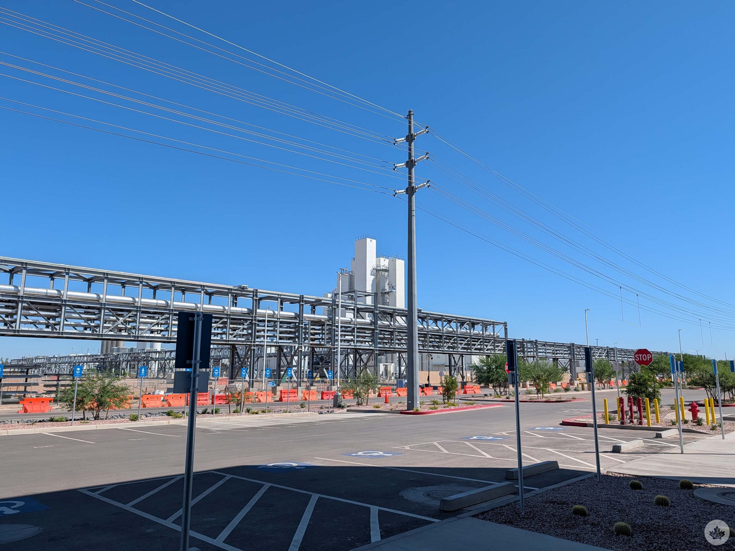
A view of the water remedy and piping on Intel’s Ocotillo campus.
The 12-acre remedy facility, a partnership between Intel Chandler, treats 9 million gallons of water per day and returns it to the manufacturing facility as a really clear water supply. Water is distributed across the Ocotillo web site by way of a water distribution loop — a few of the aforementioned piping across the buildings. Fabs use tens of millions of gallons of water each day for a variety of tasks, together with cleansing the silicon wafers used to make chips, for cooling, and extra.
Furthermore, Intel is water optimistic in Arizona, conserving water inside its operations whereas additionally funding community-based water restoration initiatives. In 2023, these initiatives restored 1.1 billion gallons (4.16 billion litres) of water to the state.
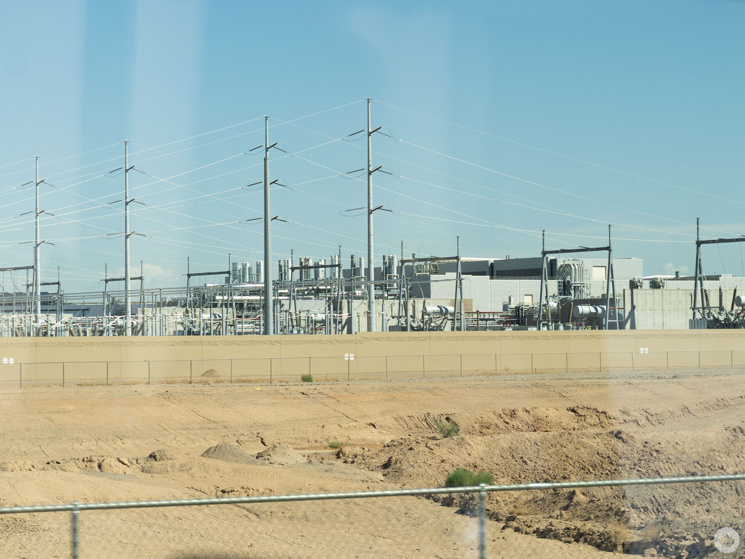
Energy era on the Ocotillo campus.
The Ocotillo campus additionally has its personal energy plant, supplying roughly 100 megawatts of electrical energy for the positioning.
Gowning as much as head inside
With the exterior tour wrapped, we headed inside to see Fab 52. The sheer scale of the power was overwhelming, particularly contemplating how small the ultimate product is. Our information famous that it’s over a mile (1.6km) throughout the entire fab, and your entire facility is walkable.
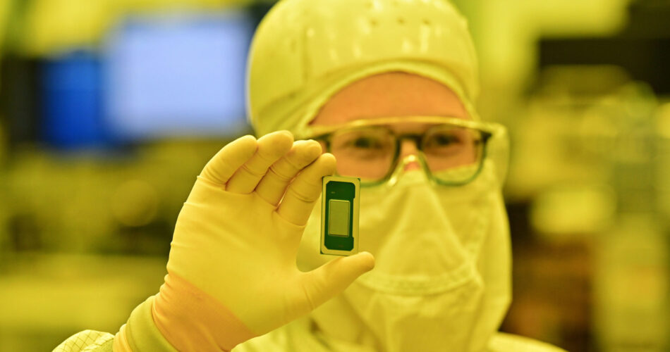
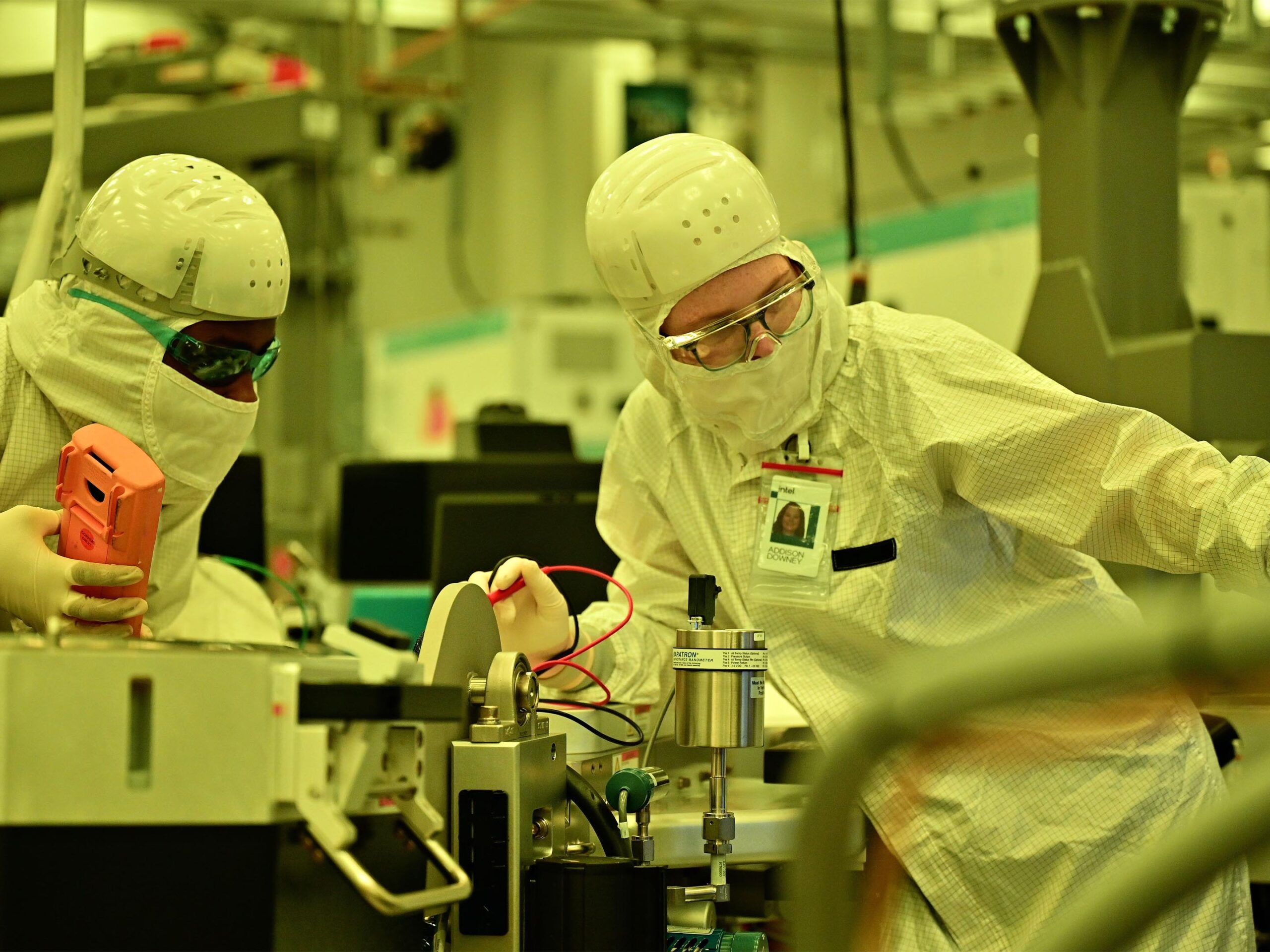
However earlier than we received inside, we needed to gear up. Fab 52, like many fabs, should be stored extremely clear as even the smallest particles of mud could be catastrophic for the fragile circuitry on pc chips.
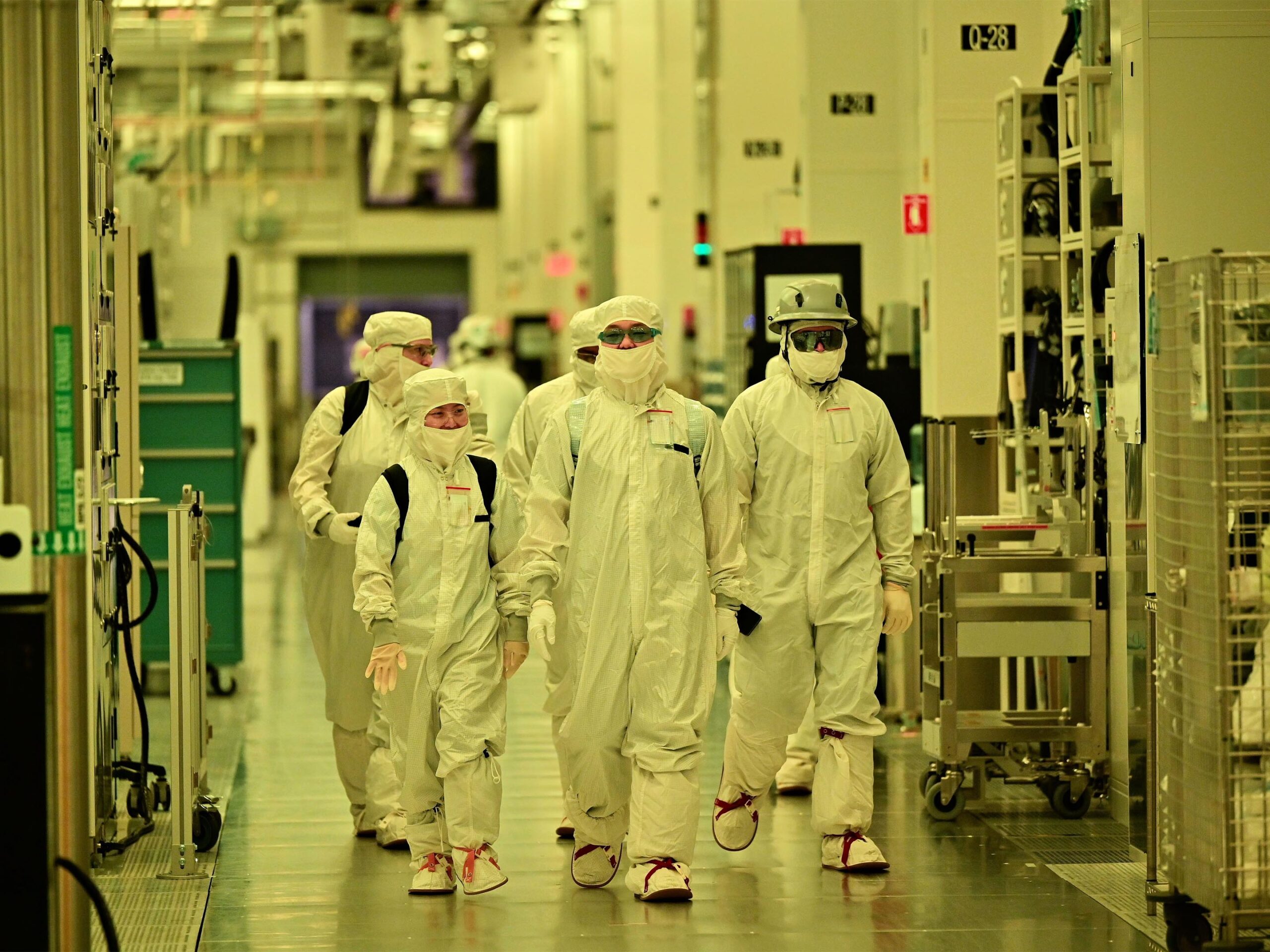
Intel staff carrying robes contained in the fab’s cleanroom setting. | Picture credit score: Intel.
Fab 52 is a category 10 clear room, which suggests it’s about 100 occasions cleaner than an working room, with air circulated six occasions per minute. Greater than that, your entire facility is designed for particular air motion, with clear air piped in by way of the ceiling and the ground composed of perforated metallic tiles that enable the air to vent out.
However mud and filth aren’t the one considerations. We couldn’t herald any wi-fi units like telephones and even smartwatches because of potential interference. Even copper was restricted, with some staff within the fab carrying pink fits to designate them as capable of work with copper to keep away from contaminating non-copper areas. Intel additionally wouldn’t enable us to herald cameras, principally because of IP safety since Intel additionally makes chips for different firms within the fab — whereas disappointing, the corporate did present ample images of the within of Fab 52, which you’ll see all through this story.
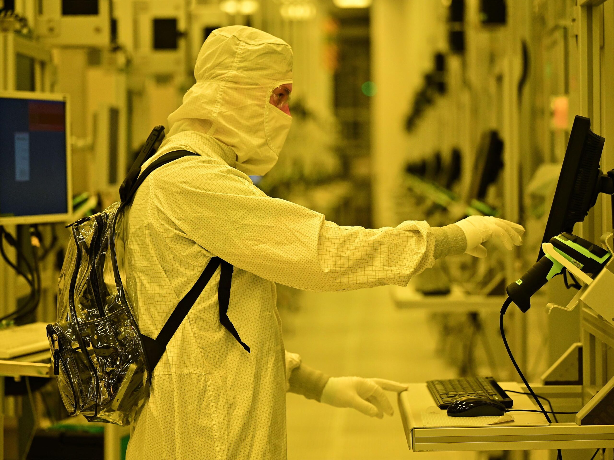
A employee completes duties on a pc inside Intel’s Fab 52. | Picture credit score: Intel.
With all of our tech securely saved, we headed as much as the fab entrance. Moving into the fab meant going by way of a sequence of doorways that felt virtually like an airlock on a spaceship. Contained in the doorways was a gowning space the place all of us needed to gown earlier than getting into the fab itself. Each one who enters should put on hair and/or beard nets, a physique go well with, a hood, two pairs of shoes, two pairs of gloves, and security glasses.
As soon as gowned, all that remained uncovered was a slim strip of our face, together with our eyes and nostril. The fits themselves weren’t cumbersome and really have been actually gentle, however with the whole lot on, they received fairly heat. Whereas we solely wore the fits for at most half-hour, those that work within the fabs put on them for hours at a time and need to de- and re-gown each time they go away the fab, resembling to make use of the washroom or to eat lunch. It took us some time to get by way of the gowning course of, however for these working within the fab, it’s virtually second nature, they usually can robe up in beneath 5 minutes.
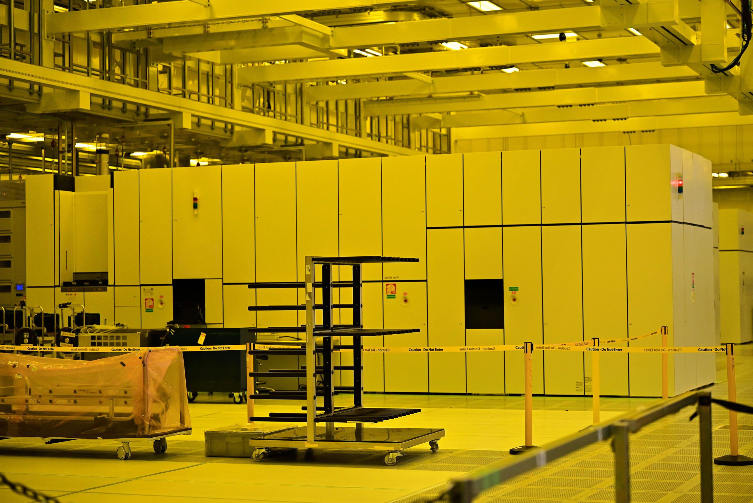
Automated methods carry silicon across the fab
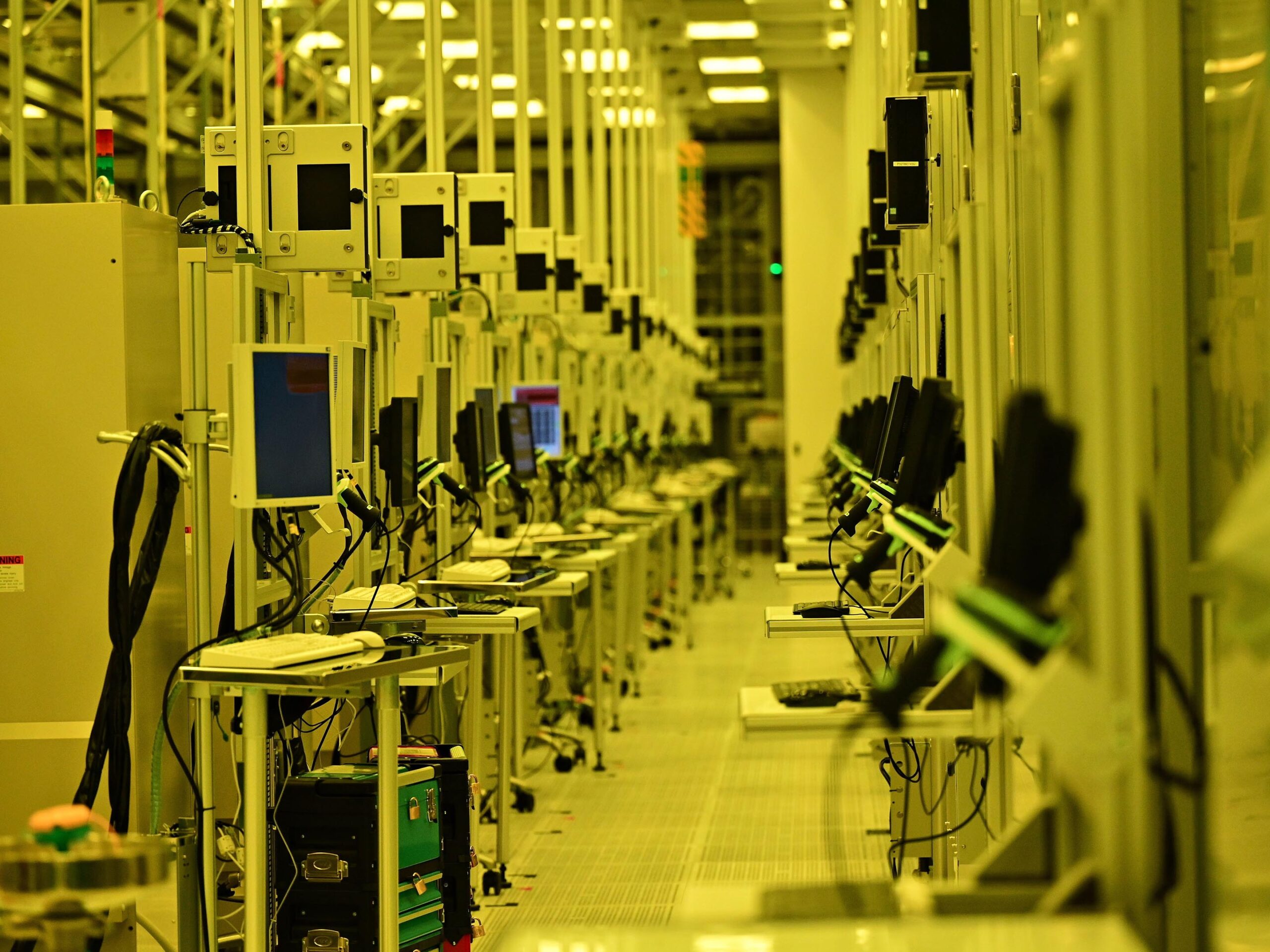
Gear inside Fab 52. | Picture credit score: Intel.
Contained in the fab was like getting into a very completely different world, a complicated future techscape. The lighting was weirdly yellow — for an excellent cause! — and all over the place I seemed, machines whirred, lights blinked, and other people suited up like me bustled. Overhead, automobiles barely bigger than your common carry-on suitcase zipped alongside on a monorail system.
The overhead monorail is a part of an automatic materials dealing with system (AMHS) that makes use of overhead hoist transports (OHTs) with front-opening unified pods (FOUPs) to hold supplies, resembling silicon wafers, across the fab. It was mesmerizing watching the AMHS in motion because the OHTs zipped alongside the rail. At intersections, the OHTs seemed about to collide, however on the final second, one would gradual barely, permitting the opposite to go safely, earlier than quickly selecting up pace once more.
Picture credit score: Intel.
Intel’s Fab 52 has over 30 miles (48.3 km) of AMHS to ship wafers on to components of the fab, like the intense ultraviolet (EUV) lithography machines. These machines are used to etch patterns on the silicon, which type the inside workings of pc chips. The video under gives an honest fundamental clarification of the chipmaking course of and even exhibits what the OHT and FOUPs seem like.
These large EUV machines can measure roughly 33 x 17 x 13 ft, weigh greater than 330,000 kilos, and cost between US$150 and US$380 million (about C$210 to C$533 million). Intel mentioned it takes 14 weeks from the arrival of those instruments till they’re capable of begin manufacturing within the fab, and the corporate makes use of particular sealed elevators to scrub the parts and transition them into the cleanroom. The EUV machines are put in in sections with specialised inflexible building to attenuate vibrations, which might additionally negatively affect the etching course of.
One of many EUV lithography machines inside Fab 52. | Picture credit score: Intel.
As talked about earlier, the fab’s odd yellow lighting is definitely an essential addition that each aids the lithography course of and boosts human imaginative and prescient. First, lithography depends on a photosensitive materials dubbed photoresist that reacts to sure wavelengths of sunshine. The yellow gentle utilized in fabs have wavelengths past the sensitivity of the photoresist, which suggests publicity to the lighting gained’t affect the lithography course of.
Furthermore, human eyes have better visibility in this type of lighting — pink lighting could make it more durable to acknowledge particulars, whereas inexperienced gentle may cause glare. The yellow lighting strikes a stability for higher visibility with out interfering with lithography and photoresist supplies.
Intel’s historical past in Arizona
An outdoor take a look at Fab 52.
Intel first began operations in Arizona again in 1979 and has since invested US$50 billion (roughly C$70 billion) in its operations there, serving to set up the area as a significant semiconductor manufacturing hub.
Intel’s Arizona campus is simply over one sq. mile in dimension and comprises a number of fabrication websites, together with:
- Fab 12, opened within the Nineteen Nineties and have become considered one of Intel’s most superior manufacturing amenities.
- Fab 22, opened in 1996.
- Fab 32, constructed within the early 2000s.
- Fab 42, accomplished in 2017.
- Fab 52, which broke floor in 2021 and is now in operation.
- Fab 62, a part of the growth that included Fab 52.
![]()
It takes three to 5 years to construct a typical fab at a price of US$20 to $25 billion (about C$28 to $35 billion). It’s not arduous to see why, with all of the tools and specialised tooling required to make chips. And once more, it’s arduous to overstate the dimensions of the infrastructure used to create these minuscule chips that energy the units we use daily.
Intel chips energy laptops, desktops, and tons of different electronics — and that’s simply Intel! There are a number of different chipmakers on the market creating silicon for tens of millions of units from smartphones to earbuds and extra. It’s somewhat bit insane how a lot goes into creating one thing most individuals use each day with out enthusiastic about it.
MobileSyrup might earn a fee from purchases made by way of our hyperlinks, which helps fund the journalism we offer free on our web site. These hyperlinks don’t affect our editorial content material. Assist us here.
Source link