

The massive image: The semiconductor business is approaching a major milestone as TSMC prepares to develop the bodily scale of its chip packaging expertise. At its current North American Expertise Symposium, the corporate detailed plans for a brand new era of CoWoS (Chip-on-Wafer-on-Substrate) expertise, enabling the meeting of multi-chiplet processors a lot bigger than these presently in manufacturing.
As we speak’s high-end processors, particularly these powering knowledge facilities and AI workloads, already depend on multi-chiplet designs to fulfill hovering calls for for efficiency and reminiscence bandwidth. TSMC’s present CoWoS options can accommodate interposers as much as 2,831 mm², greater than thrice the dimensions of a normal photomask reticle, which is proscribed to 830 – 858 mm² by EUV lithography constraints.
This expertise is already being utilized in merchandise like AMD’s Intuition MI300X and Nvidia’s B200 GPUs, which mix giant compute chipsets with stacks of high-bandwidth reminiscence.
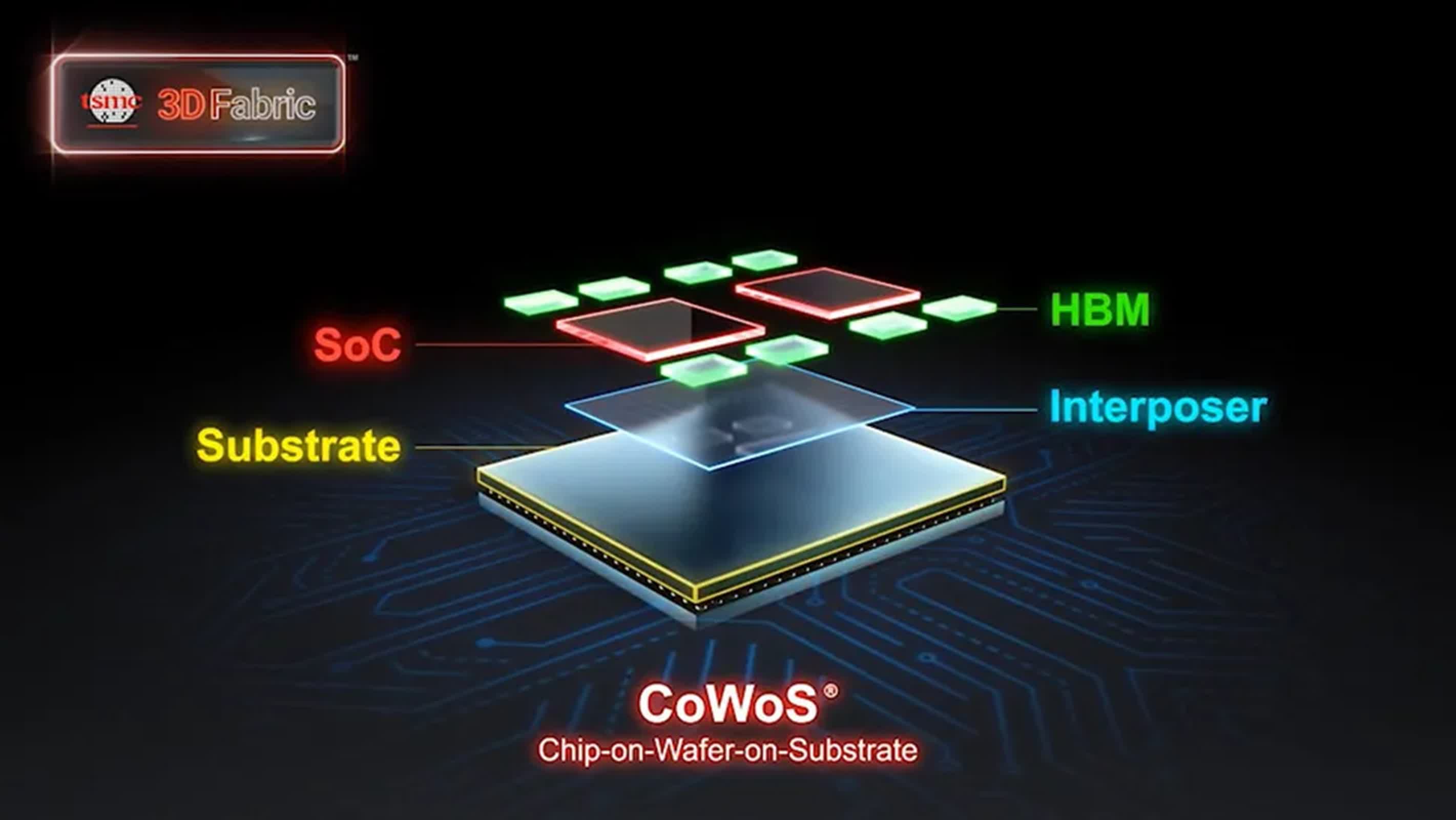
Nonetheless, as AI and high-performance computing purposes proceed to develop in complexity, the urge for food for much more silicon is barely growing. To deal with this, TSMC is developing a brand new CoWoS-L packaging expertise, set to launch as early as subsequent yr, supporting interposers as giant as 4,719 mm² – about 5.5 instances the reticle restrict – and require substrates measuring 100×100 mm. This can permit as much as 12 stacks of high-bandwidth reminiscence, a major step up from present capabilities.
TSMC initiatives that chips constructed with this expertise will ship greater than three and a half instances the compute efficiency of in the present day’s main designs, doubtlessly assembly the wants of upcoming processors like Nvidia’s Rubin GPUs.
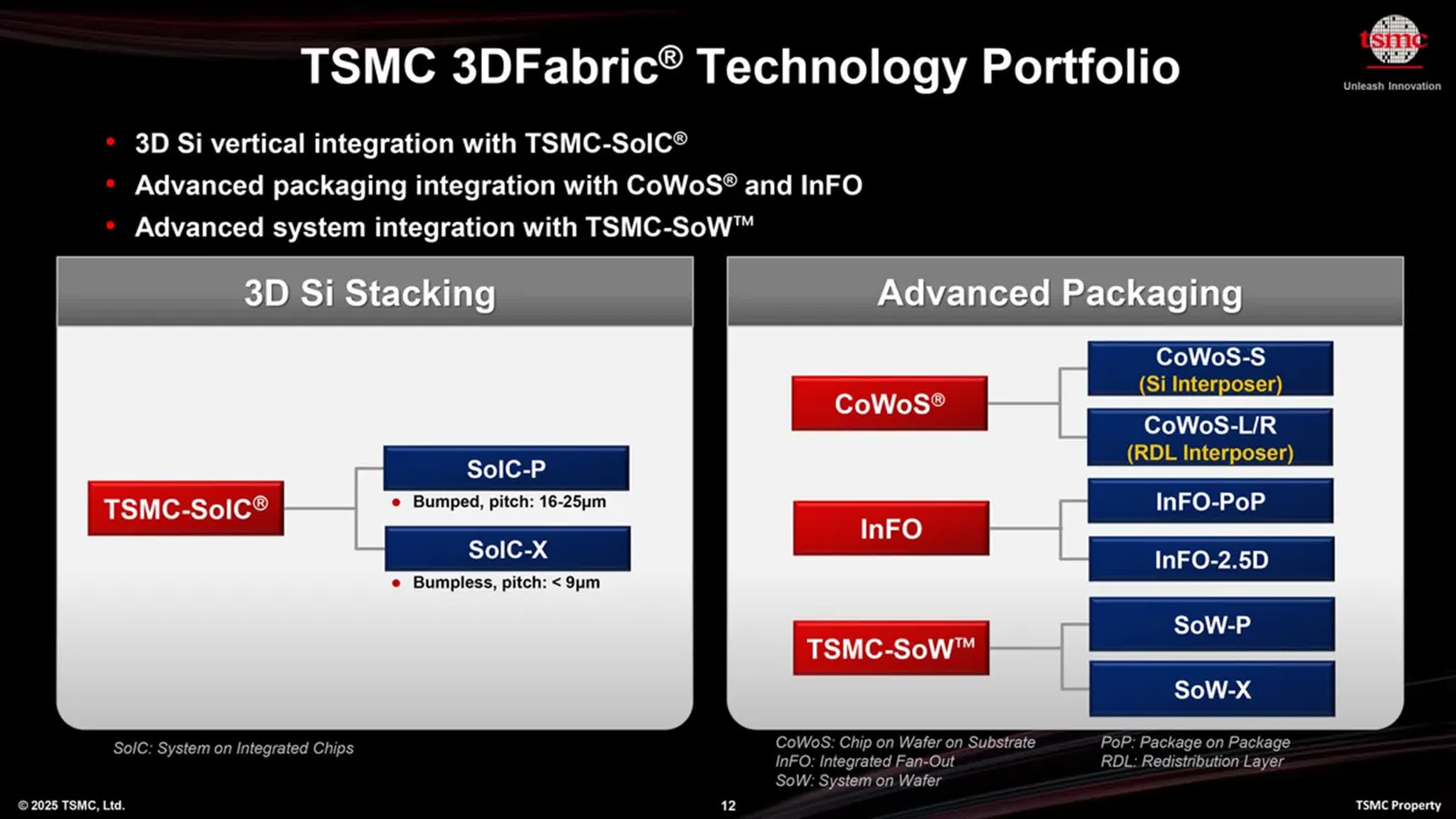
Wanting additional, TSMC plans to push the envelope with a fair bigger package deal: a 7,885 mm² interposer mounted on a 120×150 mm substrate, a footprint barely greater than a normal CD case. This represents a 9.5-fold enhance over the reticle restrict and practically doubles the realm of the corporate’s earlier 8x-reticle package deal.
Such an enormous meeting may host 4 3D-stacked systems-on-integrated chips, twelve HBM4 reminiscence stacks, and a number of enter/output dies, setting a brand new benchmark for efficiency and integration.
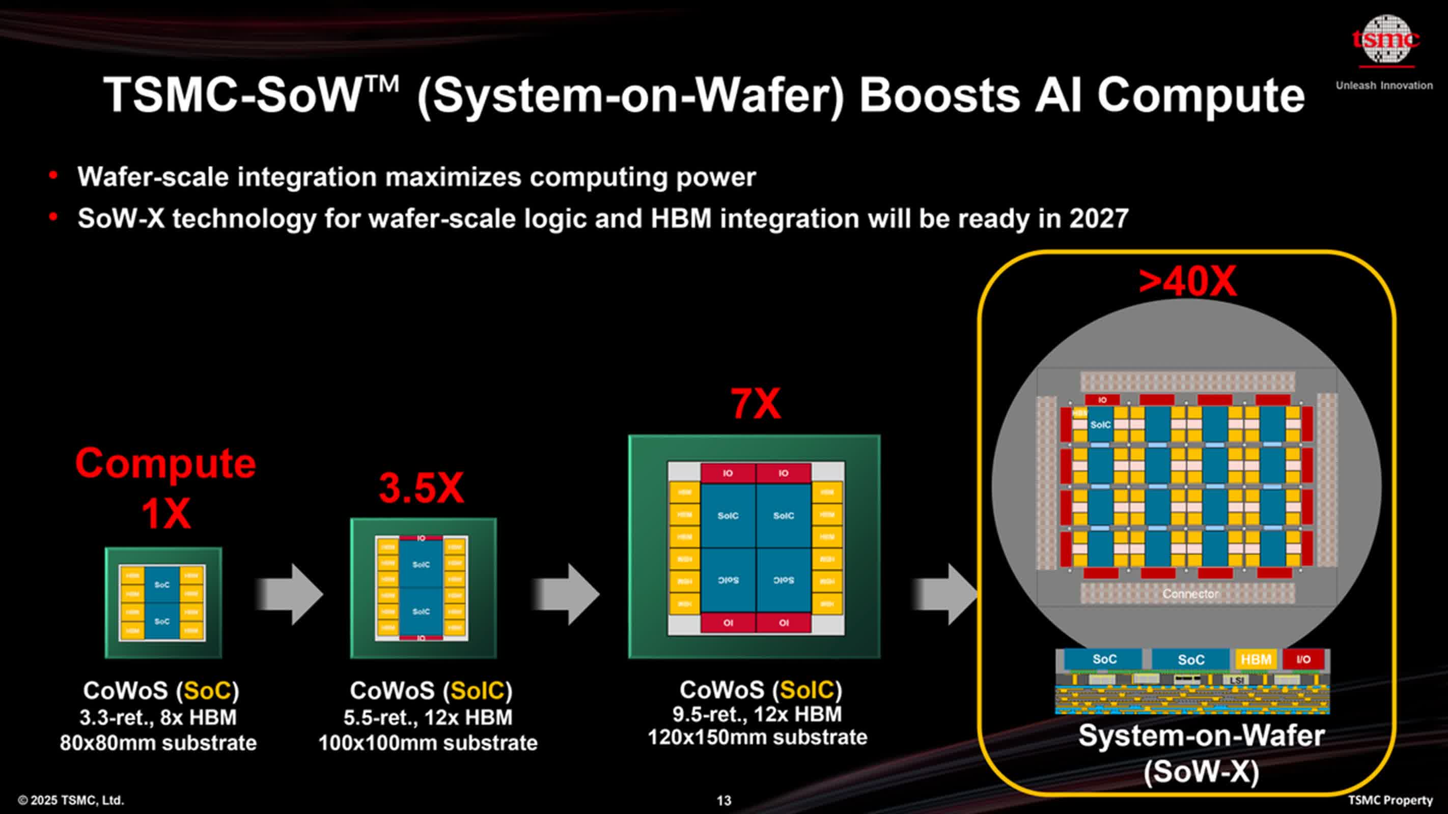
For patrons with probably the most excessive efficiency necessities, TSMC can be providing its System-on-Wafer (SoW-X) expertise, which permits the mixing of complete wafers right into a single chip. Whereas only some firms, comparable to Cerebras and Tesla, presently use wafer-level integration for specialised AI processors, TSMC anticipates broader adoption because the demand for super-sized chips grows.
The engineering challenges related to these behemoth processors are appreciable. Delivering energy to giant, multi-chiplet assemblies requires modern options, as they’ll draw kilowatts of energy, far past what conventional server designs can deal with.
To deal with this, TSMC is integrating superior energy administration circuits instantly into the chip package deal. Utilizing its N16 FinFET expertise, the corporate embeds monolithic energy administration ICs and on-wafer inductors into the CoWoS-L substrate, permitting energy to be routed effectively by the package deal.
This method reduces electrical resistance and improves energy integrity, enabling dynamic voltage scaling and fast response to altering workloads. Embedded deep trench capacitors additional stabilize electrical efficiency, filtering out voltage fluctuations and guaranteeing dependable operation below heavy computational masses.
These advances mirror a broader shift towards system-level co-optimization, the place energy supply, packaging, and silicon design are handled as interconnected components fairly than separate considerations.
Nonetheless, the transfer to ever-larger chip packages shouldn’t be with out its issues. The bodily measurement of the brand new substrates, significantly the 100×100 mm and 120×150 mm codecs, is pushing the boundaries of present module requirements comparable to OAM 2.0, and will require new system and board design approaches.

Thermal administration is one other essential problem. As processors develop in measurement and energy consumption, they generate monumental quantities of warmth. {Hardware} producers are exploring superior cooling methods, together with direct liquid cooling and immersion, to maintain these chips operating effectively.
TSMC has already labored with companions to develop immersion cooling options for knowledge facilities. These options can considerably scale back power consumption and stabilize chip temperatures, even below intense workloads. Nonetheless, integrating these cooling applied sciences instantly into chip packages stays a problem for the longer term.
Source link